LDK120
200 mA low quiescent current very low noise LDO
Datasheet - production data
Applications
• Mobile phones
• Personal digital assistants (PDAs)
627/
')1[PP
• Cordless phones and similar battery-powered
systems
• Digital still cameras
Description
The LDK120 low drop voltage regulator provides
200 mA of maximum current from an input supply
voltage in the range of 1.9 V to 5.5 V, with a
typical dropout voltage of 100 mV.
627/
It is stabilized with a ceramic capacitor on the
output.
Features
• Input voltage from 1.9 to 5.5 V
• Very low dropout voltage (100 mV typ. at 100
mA load)
• Low quiescent current (max. 100 µA, 1 µA in
OFF mode)
• Very low noise
• Output voltage tolerance: ± 2.0% @ 25 °C
The very low drop voltage, low quiescent current
and low noise features make it suitable for low
power battery-powered applications.
An enable logic control function puts the LDK120
in shutdown mode allowing a total current
consumption lower than 1 µA.
The device also includes a short-circuit constant
current limiting and thermal protection.
• 200 mA guaranteed output current
• Wide range of fixed output voltages available
on request: from 0.8 V to 3.5 V with 100 mV
step
• Adjustable version: from 0.8 V to VIN-Vdrop
• Logic-controlled electronic shutdown
• Compatible with ceramic capacitor COUT = 1 µF
• Internal current and thermal limit
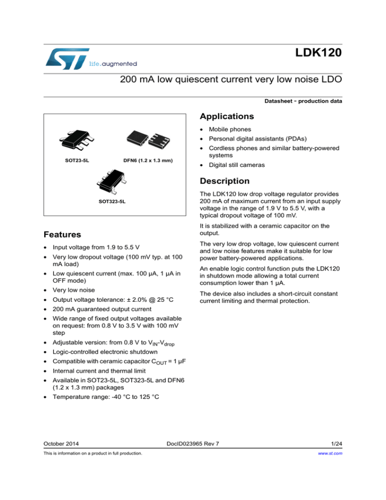
• Available in SOT23-5L, SOT323-5L and DFN6
(1.2 x 1.3 mm) packages
• Temperature range: -40 °C to 125 °C
October 2014
This is information on a product in full production.
DocID023965 Rev 7
1/24
www.st.com
24
Contents
LDK120
Contents
1
Diagram . . . . . . . . . . . . . . . . . . . . . . . . . . . . . . . . . . . . . . . . . . . . . . . . . . . 3
2
Pin configuration . . . . . . . . . . . . . . . . . . . . . . . . . . . . . . . . . . . . . . . . . . . . 4
3
Typical application . . . . . . . . . . . . . . . . . . . . . . . . . . . . . . . . . . . . . . . . . . 5
4
Maximum ratings . . . . . . . . . . . . . . . . . . . . . . . . . . . . . . . . . . . . . . . . . . . . 6
5
Electrical characteristics . . . . . . . . . . . . . . . . . . . . . . . . . . . . . . . . . . . . . 7
6
Typical performance characteristics . . . . . . . . . . . . . . . . . . . . . . . . . . . . 9
7
Package mechanical data . . . . . . . . . . . . . . . . . . . . . . . . . . . . . . . . . . . . 14
8
Packaging mechanical data . . . . . . . . . . . . . . . . . . . . . . . . . . . . . . . . . . 20
9
Order codes . . . . . . . . . . . . . . . . . . . . . . . . . . . . . . . . . . . . . . . . . . . . . . . 22
10
Revision history . . . . . . . . . . . . . . . . . . . . . . . . . . . . . . . . . . . . . . . . . . . 23
2/24
DocID023965 Rev 7
LDK120
1
Diagram
Diagram
Figure 1. Block diagram
DocID023965 Rev 7
3/24
Pin configuration
2
LDK120
Pin configuration
Figure 2. Pin connection (top view)
#:1"%+/$
SOT23-5L, SOT323-5L
DFN6 (1.2 x 1.3)
Table 1. Pin description (SOT23-5L, SOT323-5L)
Pin
Function
Symbol
SOT23/
SOT323
DFN6
1
6
IN
Input voltage of the LDO
2
2
GND
Common ground
3
4
EN
Enable pin logic input: Low = shutdown, High = active
4
3
BYP(1)/ADJ
/NC
5
1
OUT
Output voltage of the LDO
-
5
N/C
Not connected. This pin should be connected to GND
Fixed
Bypass capacitor
Adjustable
Adjustable pin
D version
Internally not connected
1. Bypass capacitor for noise reduction on fixed version is optional, if not used the relevant pin must be left
floating with no routing on the board.
4/24
DocID023965 Rev 7
LDK120
3
Typical application
Typical application
Figure 3. Typical application circuits for fixed version
287
,1
9,
(1
*1'
%<3$66
&,)
21
9R
&R)
&%<3
2))
Figure 4. Typical application circuits for D version
,1
9,
287
(1
*1'
&,)
9R
&R)
21
2))
Figure 5. Typical application circuits for adjustable version
VO=VADJ (1+R1/R2)
DocID023965 Rev 7
5/24
Maximum ratings
4
LDK120
Maximum ratings
Table 2. Absolute maximum ratings
Symbol
VIN
DC input voltage
Value
Unit
- 0.3 to 7
V
VOUT
DC output voltage
- 0.3 to VI + 0.3
V
VEN
Enable input voltage
- 0.3 to VI + 0.3
V
2
V
Output current
Internally limited
mA
Power dissipation
Internally limited
mW
VBYP/ADJ
IOUT
PD
Note:
Parameter
ADJ/Bypass pin voltage
TSTG
Storage temperature range
- 65 to 150
°C
TOP
Operating junction temperature range
- 40 to 125
°C
Absolute maximum ratings are those values beyond which damage to the device may occur.
Functional operation under these conditions is not implied. All values are referred to GND.
Table 3. Thermal data
Symbol
6/24
Parameter
SOT23-5L
SOT323-5L
DFN-6L
Unit
RthJA
Thermal resistance junction-ambient
160
246
237
°C/W
RthJC
Thermal resistance junction-case
68
134
104
°C/W
DocID023965 Rev 7
LDK120
5
Electrical characteristics
Electrical characteristics
TJ = 25 °C, VIN = VOUT(NOM) + 1 V, CIN = COUT = 1 µF, IOUT = 1 mA, VEN = VIN, unless
otherwise specified.
Table 4. Electrical characteristics for LDK120 (fixed version)
Symbol
Parameter
VIN
Operating input voltage
VOUT
VOUT accuracy
Test conditions
Min.
Typ.
Max.
Unit
1.9
5.5
V
IOUT=1 mA, TJ=25 °C
-2.0
2.0
%
IOUT=1 mA, -40 °C<TJ<125 °C
-3.0
3.0
%
ΔVOUT
Static line regulation
VOUT +1 V ≤ VIN ≤ 5.5 V, IOUT=1 mA
0.05
%/V
ΔVOUT
Static load regulation
IOUT = 1 mA to 200 mA
0.006
%/mA
VDROP
Dropout voltage
(1)
IOUT = 100 mA, VOUT=2.5 V
100
IOUT = 200 mA, VOUT=2.5 V
40 °C<TJ<125 °C
150
mV
300
eN
Output noise voltage
10 Hz to 100 kHz, IOUT=10 mA,
VOUT=2.5 V, CBYP=10 nF
51
µVRMS
eN(2)
Output noise voltage
10 Hz to 100 kHz, IOUT=10 mA,
VOUT=2.5 V
148
µVRMS
SVR
Supply voltage
rejection
VIN=VOUTNOM+0.5 V+/-VRIPPLE
VRIPPLE=0.1 V Freq.=120 Hz to 10
kHz IOUT=10 mA
55
dB
IOUT=0 mA, -40 °C<TJ<125 °C
30
60
IOUT=200 mA, -40 °C<TJ<125 °C
50
100
IQ
Quiescent current
VIN input current in OFF mode:
VEN=GND
ISC
VEN
IEN
TSHDN
COUT
Short-circuit current
RL=0
Enable input logic low
VIN=1.9 V to 5.5 V, -40 °C<TJ<125 °C
Enable input logic high
VIN=1.9 V to 5.5 V, -40 °C<TJ<125 °C
µA
1
400
mA
0.4
V
1.2
Enable pin input current VSHDN=VIN
100
Thermal shutdown
160
Hysteresis
20
nA
°C
Output capacitor
Capacitance (see Section 6: Typical
performance characteristics)
1
22
µF
1. Dropout voltage is the input-to-output voltage difference at which the output voltage is 100 mV below its nominal value.
2. Valid for D version or standard version without CBYP.
DocID023965 Rev 7
7/24
Electrical characteristics
LDK120
TJ = 25 °C, VIN = VOUT(NOM) + 1 V, CIN = COUT = 1 µF, IOUT = 1 mA, VEN = VIN, unless
otherwise specified.
Table 5. Electrical characteristics for LDK120 (adjustable version)
Symbol
Parameter
VIN
Operating input voltage
VADJ
VADJ accuracy
Test conditions
Min.
Typ.
1.9
IOUT=1 mA, TJ=25 °C
784
IOUT=1 mA, -40 °C<TJ<125 °C
-3.0
800
Max.
Unit
5.5
V
816
mV
3.0
%
ΔVOUT
Static line regulation
VOUT +1 V ≤ VIN ≤ 5.5 V, IOUT=1 mA
0.05
%/V
ΔVOUT
Static load regulation
IOUT=1 mA to 200 mA
0.006
%/mA
VDROP
eN
Dropout voltage
(1)
Output noise voltage
IADJ
Adjust pin current
SVR
Supply voltage
rejection
IQ
Quiescent current
IOUT=100 mA, VOUT=2.5 V
100
IOUT = 200 mA, VOUT=2.5 V
40 °C<TJ<125 °C,
150
10 Hz to 100 kHz, IOUT=10 mA
VOUT=VADJ
115
mV
VEN
IEN
TSHDN
COUT
µVRMS
1
VIN=VOUTNOM+0.5 V+/-VRIPPLE
VRIPPLE=0.1 V Freq.=120 Hz to 10
kHz IOUT=10 mA
55
IOUT=0 mA, -40 °C<TJ<125 °C
30
60
IOUT=200 mA, -40 °C<TJ<125 °C
50
100
VIN input current in OFF mode:
VEN=GND
ISC
300
Short-circuit current
RL=0
Enable input logic low
VIN=1.9 V to 5.5 V, -40 °C<TJ<125 °C
Enable input logic high
VIN=1.9 V to 5.5 V, -40 °C<TJ<125 °C
dB
µA
1
400
mA
0.4
V
1.2
Enable pin input current VSHDN=VIN
100
Thermal shutdown
160
Hysteresis
20
nA
°C
Output capacitor
Capacitance (see Section 6: Typical
performance characteristics)
1
22
1. Dropout voltage is the input-to-output voltage difference at which the output voltage is 100 mV below its nominal value.
8/24
µA
DocID023965 Rev 7
µF
LDK120
6
Typical performance characteristics
Typical performance characteristics
0.850
0.840
0.830
0.820
0.810
0.800
0.790
0.780
0.770
0.760
0.750
-50
AM12800v1
VIN = 1.9 V, I OUT = 1 mA
VADJ [V]
VADJ [ V ]
CIN = COUT = 1 µF, VEN to VIN, unless otherwise specified.
Figure 6. Output voltage vs. temp. for
Figure 7. Output voltage vs. temp. for
adjustable (IO = 1 mA)
adjustable version (IO = 200 mA)
-25
0
25
50
75
Temperature [°C]
100
125
150
3.500
3.400
3.300
3.200
3.100
3.000
2.900
2.800
2.700
2.600
2.500
-50
AM16198v1
VIN = 4 V, IOUT = 1 mA
-25
0
25
50
75
Temperature [°C]
100
125
150
Figure 10. Line regulation vs. temp. for
adjustable version
0
25
50
75
Temperature [°C]
100
125
150
3.500
3.400
3.300
3.200
3.100
3.000
2.900
2.800
2.700
2.600
2.500
-50
AM16199v1
VIN = 4 V, IOUT = 200 mA
-25
0
25
50
75
Temperature [°C]
100
125
150
Figure 11. Short-circuit current vs. temp. for
adjustable version
AM16201v1
600
VIN from 1.9 V to 5.5 V, I OUT = 1 mA
0.09
VIN = 1.9 V
550
0.08
500
0.07
ISHORT [mA]
Line regulation [%/V]
-25
AM16200v1
0.1
0.06
0.05
0.04
0.03
450
400
350
300
0.02
250
0.01
0
-50
AM16197v1
VIN = 1.9 V, I OUT = 200 mA
Figure 9. Output voltage vs. temp. for fixed
version (IO = 200 mA)
VOUT [V]
VOUT [V]
Figure 8. Output voltage vs. temp. for fixed
version (IO = 1 mA)
0.850
0.840
0.830
0.820
0.810
0.800
0.790
0.780
0.770
0.760
0.750
-50
-25
0
25
50
75
100
125
150
200
-50
-25
0
25
50
75
100
125
150
Temperature [°C]
Temperature [°C]
DocID023965 Rev 7
9/24
Typical performance characteristics
LDK120
Figure 12. Load regulation vs. temp. for
adjustable version
Figure 13. Load regulation vs. temp. for fixed
version
AM16202v1
0.01
AM16203v1
0.01
V IN = 4 V, I OUT from 1 mA to 200 mA
V IN = 1.9 V, I OUT from 1 mA to 200 mA
0.008
Load regulation [%/mA]
Load regulation [%/mA]
0.008
0.006
0.004
0.002
0
-50
-25
0
25
50
75
100
125
0.006
0.004
0.002
0
-50
150
-25
0
Temperature [°C]
AM16204v1
V IN = 1.9 V, I OUT = 1 mA
0.8
1.600
Low
1.400
High
1.200
0.7
0.6
0.5
0.4
-25
0
25
50
75
100
125
Low
High
1.000
0.800
0.600
0.000
-50
150
-25
0
50
75
100
125
150
Figure 17. Quiescent current vs. temp. for
adjustable version (IO = 200 mA)
AM16207v1
200
V IN = 1.9 V, I OUT = 0 mA
90
25
Temperature [°C]
AM16206v1
100
V IN = 1.9 V, I OUT = 200 mA
180
80
Quiescent current [µA]
Quiescent current [µA]
150
0.200
Figure 16. Quiescent current vs. temp. for
adjustable version (IO = 0 mA)
70
60
50
40
30
20
160
140
120
100
80
60
40
20
10
10/24
125
AM16205v1
V IN = 5.5 V, I OUT = 1 mA
Temperature [°C]
0
-50
100
0.400
0.3
0.2
-50
75
Figure 15. Enable pin thresholds vs. temp.
V EN Thresholds [V]
VEN Thresholds [V]
0.9
50
Temperature [°C]
Figure 14. Enable pin thresholds vs. temp.
(VIN = 1.9 V)
1
25
-25
0
25
50
75
Temperature [ °C]
100
125
150
0
-50
-25
0
25
50
75
Temperature [°C]
DocID023965 Rev 7
100
125
150
LDK120
Typical performance characteristics
Figure 18. Quiescent current vs. temp. for fixed Figure 19. Quiescent current vs. temp. for fixed
version (IO = 0 mA)
version (IO = 200 mA)
AM16208v1
100
V IN = 4 V, I OUT = 0 mA
V IN = 4 V, I OUT = 200 mA
180
80
Quiescent current [µA]
Quiescent current [µA]
AM16209v1
200
90
70
60
50
40
30
20
160
140
120
100
80
60
40
20
10
0
-50
-25
0
25
50
75
100
125
0
-50
150
-25
0
25
Temperature [°C]
Figure 20. Shutdown current vs. temperature
150
AM16211v1
70
No Cbyp
60
0.7
50
0.6
SVR [dB]
Quiescent current [µA]
125
Cbyp =10 nF
0.8
0.5
0.4
0.3
40
30
20
0.2
10
0.1
0
-50
100
80
V IN = 4 V , V EN = GND
0.9
75
Figure 21. SVR vs. frequency (VO = 2.5 V)
AM16210v1
1
50
Temperature [°C]
V OUT = 2.5 V, VIN = VOUT + 0.5 V +/ - 100 mV, I OUT = 10 mA
-25
0
25
50
75
100
125
0
100
150
1000
10000
100000
Frequency [Hz]
Temperature [°C]
Figure 22. SVR vs. frequency (VO = VADJ)
Figure 23. Output noise vs. frequency
(VO = 3.3 V)
AM16213v1
AM16212v1
80
1.4
Cbyp = 10 nF
No Cbyp
70
1.2
eN [µV /Sqrt (Hz)]
60
SVR [dB]
VIN = 4.3 V, IOUT = 10 mA
50
40
30
20
10
1
0.8
0.6
0.4
0.2
VOUT = V ADJ, VIN = VOUT + 0.5 V +/ - 100 mV, I OUT = 10 mA
0
100
1000
10000
Frequency [Hz]
100000
0
1000
10000
100000
Frequency (Hz)
DocID023965 Rev 7
11/24
Typical performance characteristics
LDK120
Figure 24. Output noise vs. frequency
(VO = VADJ)
Figure 25. Stability region vs. COUT (fixed)
AM16214v1
VIN = 1.8 V, IOUT = 10 mA
9
1.2
8
1.0
7
ESR @ 100 kHz [Ω]
eN [µV /Sqrt (Hz)]
AM16215v1
10
1.4
0.8
0.6
0.4
6
Stability area
5
4
3
2
0.2
1
0
0.0
1000
10000
100000
0
1
2
3
4
5
6
7
8
9 10 11 12 13 14 15 16 17 18 19 20 21 22 23
COUT [µF] (nominal value)
Frequency [Hz]
VIN = VEN = 4 to 5.5 V, IOUT = 10 mA to 0.2 A, CIN = 1 µF,
TA = 25 °C
Figure 26. Stability region vs COUT (adjust.)
Figure 27. Line transient (VOUT = VADJ)
AM16216v1
10
9
8
ESR @ 100 kHz [Ω]
7
6
Stability area
5
4
3
2
1
0
0
1
2
3
4
5
6
7
8
9 10 11 12 13 14 15 16 17 18 19 20 21 22 23
COUT [µF] (nominal value)
VIN = VEN = 1.9 to 5.5 V, IOUT = 10 mA to 0.2 A, CIN = 1 µF,
TA = 25 °C
Figure 28. Line transient (VOUT = 3 V)
VOUT = 3 V, VIN = 4 V to 4.5 V, VEN = 2 V, IOUT = 1 mA, NO
CIN, COUT = 1 µF, tr = tf = 5 µs
12/24
VOUT = VADJ, VIN = 3.5 V to 4 V, VEN = 2 V, IOUT = 1 mA, NO
CIN, COUT = 1 µF, tr = tf = 5 µs
Figure 29. Load transient (VOUT = 3 V)
VOUT = 3 V, VIN = VEN = 3.5 V, IOUT = 1 mA to 200 mA, COUT
= 1 µF, tr = tf = 5 µs
DocID023965 Rev 7
LDK120
Typical performance characteristics
Figure 30. Load transient (VOUT = VADJ)
Figure 31. Startup transient
VOUT = VADJ, VIN = VEN = 3.5 V, IOUT = 1 mA to 200 mA,
COUT = 1 µF, tr = tf = 5 µs
VOUT = 3 V, VIN = VEN = 0 to 4.2 V, IOUT = 1 mA, CIN = COUT
= 1 µF, tr = tf = 5 µs
Figure 32. Enable transient (VOUT = VADJ)
Figure 33. Enable transient (VOUT = 3 V)
VIN = 4 V, VEN = 0 to VIN, IOUT = 200 mA, CIN = COUT = 1 µF,
tr = tf = 1 µs
VOUT @ 0.8 V, VIN = 1.9, VEN = 0 to VIN, IOUT = 200 mA,
COUT = 1 µF, tr = tf = 1 µs
Figure 34. Dropout voltage vs. temperature
(IOUT = 100 mA)
Figure 35. Dropout voltage vs. temperature
(IOUT = 200 mA)
AM16226v1
300
C IN = COUT = 1 µF, IOUT = 200 mA, Fixed 3.0 V version
250
Dropout Voltage [mV]
Dropout Voltage [mV]
250
200
150
100
50
0
-50
AM16227v1
300
C IN = COUT = 1 µF, IOUT = 100 mA, Fixed 3.0 V version
-25
0
25
50
75
100
125
150
200
150
100
50
0
-50
-25
0
25
50
75
100
125
150
Temperature [°C]
Temperature [ °C]
DocID023965 Rev 7
13/24
Package mechanical data
7
LDK120
Package mechanical data
In order to meet environmental requirements, ST offers these devices in different grades of
ECOPACK® packages, depending on their level of environmental compliance. ECOPACK
specifications, grade definitions and product status are available at: www.st.com.
ECOPACK is an ST trademark.
Figure 36. SOT23-5L mechanical drawing
BN
14/24
DocID023965 Rev 7
LDK120
Package mechanical data
Table 6. SOT23-5L mechanical data
mm
Dim.
Min.
Typ.
Max.
A
0.90
1.45
A1
0
0.15
A2
0.90
1.30
b
0.30
0.50
c
0.09
0.20
D
2.95
E
1.60
e
0.95
H
2.80
L
0.30
0.60
θ
0
8
Figure 37. SOT23-5L footprint (dimensions in mm)
BN
DocID023965 Rev 7
15/24
Package mechanical data
LDK120
Figure 38. DFN6L (1.2 x 1.3 mm) drawing
B$
16/24
DocID023965 Rev 7
LDK120
Package mechanical data
Table 7. DFN6L (1.2 x 1.3 mm) mechanical data
mm
Dim.
Min.
Typ.
Max.
A
0.41
0.45
0.50
A1
0.00
0.02
0.05
D
-
1.20
-
E
-
1.30
-
e
-
0.40
-
b
0.15
0.18
0.25
L
0.475
0.525
0.575
L3
0.375
0.425
0.475
aaa
-
0.05
-
Figure 39. DFN6L footprint (dimensions in mm)
B$
DocID023965 Rev 7
17/24
Package mechanical data
LDK120
Figure 40. SOT323-5L drawing
BI
18/24
DocID023965 Rev 7
LDK120
Package mechanical data
Table 8. SOT323-5L mechanical data
mm
Dim.
Min.
Typ.
Max.
A
0.80
1.10
A1
0
0.10
A2
0.80
b
0.15
0.30
c
0.10
0.22
D
1.80
2
2.20
E
1.80
2.10
2.40
E1
1.15
1.25
1.35
0.90
e
0.65
e1
1.30
L
0.26
<
0°
DocID023965 Rev 7
0.36
1
0.46
8°
19/24
Packaging mechanical data
8
LDK120
Packaging mechanical data
Figure 41. SOT23-5L and SOT323-xL tape and reel drawing
20/24
DocID023965 Rev 7
LDK120
Packaging mechanical data
Table 9. SOT23-5L tape and reel mechanical data
mm
Dim.
Min.
Typ.
A
Max.
180
C
12.8
D
20.2
N
60
13.0
T
13.2
14.4
Ao
3.13
3.23
3.33
Bo
3.07
3.17
3.27
Ko
1.27
1.37
1.47
Po
3.9
4.0
4.1
P
3.9
4.0
4.1
Table 10. SOT323-xL tape and reel mechanical data
mm
Dim.
Min.
Typ.
Max.
A
175
180
185
C
12.8
13
13.2
D
20.2
N
59.5
60
60.5
T
14.4
Ao
2.25
Bo
3.17
Ko
1.2
Po
3.9
4.0
4.1
P
3.9
4.0
4.2
DocID023965 Rev 7
21/24
Order codes
9
LDK120
Order codes
Table 11. Order codes
Package
Output
voltage
SOT323-5L
SOT23-5L
DFN6L
LDK120C-R
LDK120M-R
LDK120PU-R
ADJ
LDK120C08R
LDK120M08R
LDK120PU08R
0.8 V
LDK120C10R
LDK120M10R
LDK120PU10R
1.0 V
LDK120C11R
LDK120M11R
LDK120C12R
LDK120M12R
LDK120C15R
LDK120M15R
LDK120C18R
LDK120M18R
LDK120PU18R
1.8 V
LDK120C25R
LDK120M25R
LDK120PU25R
2.5 V
LDK120C28R
LDK120M28R
LDK120C29R
LDK120M29R
LDK120PU29R
2.9 V
LDK120C30R
LDK120M30R
LDK120PU30R
3.0 V
LDK120C31R
LDK120M31R
LDK120C32R
LDK120M32R
1.1 V
LDK120PU12R
1.5 V
2.8 V
3.1 V
LDK120PU32R
LDK120DM33R
LDK120C33R
LDK120M33R
1.2 V
3.2 V
3.3 V
LDK120PU33R
LDK120C35R
3.3 V
3.5 V
Table 12. Marking
22/24
Order codes
Package
Output voltage
Marking
LDK120DMxxR
SOT23-5L
xx V
Dxx
LDK120MxxR
SOT23-5L
xx V
Kxx
LDK120CxxR
SOT323-5L
xx V
Kxx
LDK120PUxxR
DFN-6L
xx V
xx
LDK120M-R
SOT23-5L
Adj
KAD
LDK120C-R
SOT323-5L
Adj
KAD
LDK120PU-R
DFN-6L
Adj
AD
DocID023965 Rev 7
LDK120
10
Revision history
Revision history
Table 13. Document revision history
Date
Revision
Changes
26-Nov-2012
1
Initial release
31-Jan-2013
2
Added new part number LDK120PU32R
Updated Table 11 on page 22
18-Oct-2013
3
RPN LDK120xx changed to LDK120.
Updated the Features and the Description in cover page.
Cancelled Table1: Device summary.
Updated Section 7: Package mechanical data, Table 2: Absolute
maximum ratings and Table 11: Order codes.
Added Section 8: Packaging mechanical data.
Minor text changes.
10-Mar-2014
4
Updated Table 11: Order codes.
29-Apr-2014
5
Updated Table 1: Pin description (SOT23-5L, SOT323-5L), Table 4:
Electrical characteristics for LDK120 (fixed version), Table 5:
Electrical characteristics for LDK120 (adjustable version), Table 11:
Order codes and Table 12: Marking.
Added Figure 4: Typical application circuits for D version.
Minor text changes.
29-Aug-2014
6
Updated Table 6: SOT23-5L mechanical data and Table 11: Order
codes.
07-Oct-2014
7
Updated Table 11: Order codes.
Minor text changes.
DocID023965 Rev 7
23/24
LDK120
IMPORTANT NOTICE – PLEASE READ CAREFULLY
STMicroelectronics NV and its subsidiaries (“ST”) reserve the right to make changes, corrections, enhancements, modifications, and
improvements to ST products and/or to this document at any time without notice. Purchasers should obtain the latest relevant information on
ST products before placing orders. ST products are sold pursuant to ST’s terms and conditions of sale in place at the time of order
acknowledgement.
Purchasers are solely responsible for the choice, selection, and use of ST products and ST assumes no liability for application assistance or
the design of Purchasers’ products.
No license, express or implied, to any intellectual property right is granted by ST herein.
Resale of ST products with provisions different from the information set forth herein shall void any warranty granted by ST for such product.
ST and the ST logo are trademarks of ST. All other product or service names are the property of their respective owners.
Information in this document supersedes and replaces information previously supplied in any prior versions of this document.
© 2014 STMicroelectronics – All rights reserved
24/24
DocID023965 Rev 7
