EE 322 Advanced Electronics, Spring 2012 Homework #2 solution
advertisement
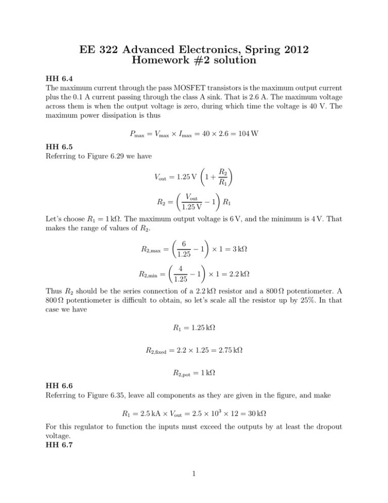
EE 322 Advanced Electronics, Spring 2012 Homework #2 solution HH 6.4 The maximum current through the pass MOSFET transistors is the maximum output current plus the 0.1 A current passing through the class A sink. That is 2.6 A. The maximum voltage across them is when the output voltage is zero, during which time the voltage is 40 V. The maximum power dissipation is thus Pmax = Vmax × Imax = 40 × 2.6 = 104 W HH 6.5 Referring to Figure 6.29 we have R2 Vout = 1.25 V 1 + R1 Vout − 1 R1 R2 = 1.25 V Let’s choose R1 = 1 kΩ. The maximum output voltage is 6 V, and the minimum is 4 V. That makes the range of values of R2 . 6 R2,max = − 1 × 1 = 3 kΩ 1.25 4 R2,min = − 1 × 1 = 2.2 kΩ 1.25 Thus R2 should be the series connection of a 2.2 kΩ resistor and a 800 Ω potentiometer. A 800 Ω potentiometer is difficult to obtain, so let’s scale all the resistor up by 25%. In that case we have R1 = 1.25 kΩ R2,fixed = 2.2 × 1.25 = 2.75 kΩ R2,pot = 1 kΩ HH 6.6 Referring to Figure 6.35, leave all components as they are given in the figure, and make R1 = 2.5 kA × Vout = 2.5 × 103 × 12 = 30 kΩ For this regulator to function the inputs must exceed the outputs by at least the dropout voltage. HH 6.7 1 Design an adjustable current source for output currents from 10 µA to 10 mA using a 317. If Vin = +15 V, what is the output compliance? Assume a dropout voltage of 2 V. We will use the circuit in Figure 6.38B. We will use two resistors, one fixed and one adjustable. Vin R1 LM 317 R2 + Iout − The voltage between the output pin and the adjust pin is Vref = 1.25 V. The output current is then Vref R1 + R2 The maximum current flows when the resistance is minimized, Iout = Iout,max = Vref R1 So that R1 = Vref Iout,max = 1.25 = 1.25 kΩ 1 × 10⁻³ The minimum current flows when the resistance is maximized, Iout,min = Vref R1 + R2 So that R2 = Vref Iout,min − R1 = 1.25 − 1.25 × 103 = 123 kΩ 10 × 10−6 We can thus achieve the currents we want by using a 1.25 kΩ resistor, R1 , in series with a 0 − 123 kΩ potentiometer, R2 . The compliance voltage range is the range of voltages on the output pin over which these currents can flow. The highest current is the most restrictive current. The maximum voltage on the output pin consistent with a 15 V input, and drop-out voltage of 2 V, and the voltage drop across feedback resistors is 2 Vout,max =Vin − Vdropout − Vref =15 − 2 − 1.25 =11.75 V 3
