EN71PL03280 Purpose Eon products` New Top Marking Continuity
advertisement

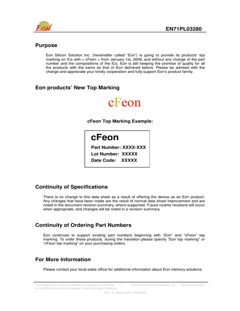
EN71PL03280 Purpose Eon Silicon Solution Inc. (hereinafter called “Eon”) is going to provide its products’ top marking on ICs with < cFeon > from January 1st, 2009, and without any change of the part number and the compositions of the ICs. Eon is still keeping the promise of quality for all the products with the same as that of Eon delivered before. Please be advised with the change and appreciate your kindly cooperation and fully support Eon’s product family. Eon products’ New Top Marking cFeon Top Marking Example: cFeon Part Number: XXXX-XXX Lot Number: XXXXX Date Code: XXXXX Continuity of Specifications There is no change to this data sheet as a result of offering the device as an Eon product. Any changes that have been made are the result of normal data sheet improvement and are noted in the document revision summary, where supported. Future routine revisions will occur when appropriate, and changes will be noted in a revision summary. Continuity of Ordering Part Numbers Eon continues to support existing part numbers beginning with “Eon” and “cFeon” top marking. To order these products, during the transition please specify “Eon top marking” or “cFeon top marking” on your purchasing orders. For More Information Please contact your local sales office for additional information about Eon memory solutions. This Data Sheet may be revised by subsequent versions 1 or modifications due to changes in technical specifications. ©2004 Eon Silicon Solution, Inc., Rev. A, Issue Date: 2009/10/6 www.eonssi.com EN71PL03280 EN71PL032 Base MCP Stacked Multi-Chip Product (MCP) Flash Memory and RAM 32 Megabit (2M x 16-bit) CMOS 3.0 Volt-only Simultaneous Operation Page Mode Flash Memory and 8 Megabit (512K x 16-bit) Pseudo Static RAM Distinctive Characteristics MCP Features Power supply voltage of 2.7 V to 3.3V High performance - 70 ns Package - 7 x 9 x 1.2mm 56 ball FBGA Operating Temperature - 25°C to +85°C General Description The EN71PL series is a product line of stacked Multi-Chip Product (MCP) packages and consists of: EN29PL032 (Simultaneous Read/Write) Flash memory die. Pseudo SRAM. For detailed specifications, please refer to the individual datasheets listed in the following table. Device Document NOR Flash EN29PL032 Pseudo SRAM ENPSL80 Product Selector Guide 32Mb Flash Memory Device-Model# EN71PL03280 pSRAM density 8M pSRAM Flash Access time 70ns pSRAM Access time 70ns Page read Access time 25ns Package pSRAM Page read Access time 25ns 56 FBGA MCP Block Diagram This Data Sheet may be revised by subsequent versions 2 or modifications due to changes in technical specifications. ©2004 Eon Silicon Solution, Inc., Rev. A, Issue Date: 2009/10/6 www.eonssi.com EN71PL03280 Connection Diagram This Data Sheet may be revised by subsequent versions or modifications due to changes in technical specifications. 3 ©2004 Eon Silicon Solution, Inc., Rev. A, Issue Date: 2009/10/6 www.eonssi.com EN71PL03280 MCP Flash-only Addresses Shared Addresses EN71PL03280 A20, A19 A18 – A0 Note: A9 = VID for HV Autoselect mode is not available for MCP product. This Data Sheet may be revised by subsequent versions or modifications due to changes in technical specifications. 4 ©2004 Eon Silicon Solution, Inc., Rev. A, Issue Date: 2009/10/6 www.eonssi.com EN71PL03280 Pin Description Signal Description A20–A0 21 Address Inputs (Common) DQ15–DQ0 16 Data Inputs/Outputs (Common) CE1#f Chip Enable 1 (Flash) CE1#ps Chip Enable 1 (pSRAM) CE2ps Chip Enable 2 (pSRAM) OE# Output Enable (Common) WE# Write Enable (Common) RY/BY# Ready/Busy Output (Flash) UB# Upper Byte Control (pSRAM) LB# Lower Byte Control (pSRAM) RESET# Hardware Reset Pin, Active Low (Flash) WP#/ACC Hardware Write Protect/Acceleration Pin (Flash) VCCf Flash 3.0 volt-only single power supply VCCps pSRAM Power Supply VSS Device Ground (Common) NC Pin Not Connected Internally Note: A9 = VID for HV Autoselect mode is not available for MCP product. Logic Symbol This Data Sheet may be revised by subsequent versions or modifications due to changes in technical specifications. 5 ©2004 Eon Silicon Solution, Inc., Rev. A, Issue Date: 2009/10/6 www.eonssi.com EN71PL03280 ORDERING INFORMATION EN71PL032 80 70 C W P PACKAGING CONTENT (Blank) = Conventional P = Pb Free TEMPERATURE RANGE W = Wireless (-25°C to +85°C) PACKAGE C =56-Ball Fine Pitch Ball Grid Array (FBGA) 0.80mm pitch, 7mm x 9mm package SPEED 70 = 70ns pSRAM density 80 = 8M pSRAM BASE PART NUMBER EN = Eon Silicon Solution Inc. 71PL = Multi-chip Product (MCP) 3.0V Simultaneous Read/Write, Page Mode Flash Memory and RAM 032 = 32 Megabit (2M x 16) This Data Sheet may be revised by subsequent versions or modifications due to changes in technical specifications. 6 ©2004 Eon Silicon Solution, Inc., Rev. A, Issue Date: 2009/10/6 www.eonssi.com EN71PL03280 PACKAGE MECHANICAL 56-ball Fine-Pitch Ball Grid Array (FBGA) 7 x 9 mm Package, pitch: 0.8mm, ball: 0.4mm SYMBOL DIMENSION IN MM MIN. NOR MAX A - -- --- 1.20 A1 0.25 0.30 0.35 A2 0.80 --- 0.95 D E 8.95 6.95 9.00 7.00 9.05 7.05 D1 - -- 5.60 - -- E1 - -- 5.60 - -- e b - -0.35 0.80 0.40 - -0.45 Note : Controlling dimensions are in millimeters (mm). This Data Sheet may be revised by subsequent versions or modifications due to changes in technical specifications. 7 ©2004 Eon Silicon Solution, Inc., Rev. A, Issue Date: 2009/10/6 www.eonssi.com EN71PL03280 Revisions List Revision No Description Date A Initial Release 2009/05/05 B Update package mechanical dimension in page 7 2009/10/06 This Data Sheet may be revised by subsequent versions or modifications due to changes in technical specifications. 8 ©2004 Eon Silicon Solution, Inc., Rev. A, Issue Date: 2009/10/6 www.eonssi.com


