Fly-back
transformer design instructions
Design tool
1. Overview
This material describes how to design the transformer for Fly-back type power supply. It describes the
using method of the Excel file provided as a transformer design tool.
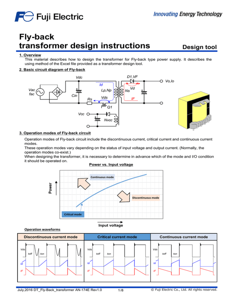
2. Basic circuit diagram of Fly-back
D1,VF
Vdc
Vo,Io
Id
Vac
fac
Lp,Np
Cin
Ns
Vds
Rs
Vd
IF
Q1
Vcc
Nvcc
3. Operation modes of Fly-back circuit
Operation modes of Fly-back circuit include the discontinuous current, critical current and continuous current
modes.
These operation modes vary depending on the status of input voltage and output current. (Normally, the
operation modes co-exist.)
When designing the transformer, it is necessary to determine in advance which of the mode and I/O condition
it should be operated on.
Power vs. Input voltage
Power
Continuous mode
Discontinuous mode
Critical mode
Input voltage
Operation waveforms
Discontinuous current mode
Vds
Critical current mode
Vds
toff
ton
Continuous current mode
Vds
toff
ton
toff
Id
Id
Id
IF
IF
IF
July,2016 DT_Fly-Back_transformer AN-174E Rev1.0
1 /8
ton
© Fuji Electric Co., Ltd. All rights reserved.
Fly-back transformer Design
4. Parameters required to design transformer
Item
Power
supply
specification
Using part
Using core
Usage
condition
Symbol
Unit
Output voltage
Vo
Vdc
Rated output current (max.)
Io
Adc
Overload protection operating current
Iolp
Adc
Input voltage
Vac
Vac
Min,Max
Input frequency
fac
Hz
Min
Conversion efficiency
η
%
Switching frequency
fsw
kHz
Input capacitance of the electrolytic
capacitor
Cin
uF
Secondary side diode VF
VF
Vdc
Used maximum magnetic flux density
⊿B
T
Effective magnetic path length of core
le
mm2
Effective cross-section area of core
Ae
Mm
Relative permeability (amplitude
permeability)
μa
Fly-back voltage
Vr
Vdc
MOSFET surge voltage (estimate)
Vsgm
Vdc
Diode surge voltage at secondary side
(estimate)
Vsgd
Vdc
Vin(cr),
Vin(cc)
Adc
Output current when setting operation
mode
Io(cr),
Io(cc)
Adc
Continuity level when setting operation
mode
(For continuous mode only)
k
Input voltage when setting operation mode
Required condition
5. Parameters to be calculated
Item
Output power
Ripple voltage (estimate)
Unit
Po
W
Po,Polp
Vripple
Vdc
Vripple,Vripple(olp)
Minimum input voltage
Vdc(min)
Vdc
Vdc(min),Vdcolp)min)
Maximum input voltage
Vdc(max)
Vdc
Input current
Switching cycle
Calculating
parameters
Symbol
Pin
W
Pin,Pinolp
T
us
T,Ton
Maximum MOSFET voltage
Vds(max)
Vdc
Maximum diode voltage at secondary side
Vd(max)
Vdc
Duty
D
Primary side inductance
Lp
uH
Number of turns at primary side
Np
Tn
Number of turns at secondary side
Number of turns of VCC
Core gap length
Ns
Tn
Nvcc
Tn
lg
mm
Peak current at primary side
Ipeak
A
Current at primary side (effective value)
Iprms
Arms
Current at secondary side (effective value)
Isrms
Arms
Output capacitor current (effective value)
Icrms
Arms
Bc
T
Magnetic flux density in core
July,2016 DT_Fly-Back_transformer AN-174E Rev1.0
2 /8
© Fuji Electric Co., Ltd. All rights reserved.
Fly-back transformer Design
6. Design flow of transformer for Fly-back
Step
Item
Description
Step-0
Determine operation mode
Determine whether the critical mode (discontinuous
mode) or continuous mode should be used for the
design.
Step-1
Determine parameters
Temporarily determine the power supply specification
and using parts.
Step-2
Determine Fly-back voltage
Determine the Fly-back voltage based on breakdown
voltages of the MOSFET to be used and diode at the
secondary side.
Step-3
Determine turns ratio
The turns ratio is determined based on the Fly-back
voltage.
Step-4
Operation condition under critical
or continuous mode
Step-5
Calculate Duty and Lp
Calculate Duty and Lp under the operation condition of
Step-4.
Step-6
Calculate D(max) on OLP
Obtain the maximum Duty for the power supply
specification.
Step-7
Calculate Ipeak
Obtain the maximum current Ipeak flowing through the
primary side with Lp set in Step-4 under the maximum
Duty condition.
Step-8
Determine number of turns at
secondary side (Ns)
Calculate the number of turns at the secondary side (Ns)
based on the specification of core to be used, LP and
Ipeak.
Step-9
Determine number of turns at
primary side (Np)
Calculate the number of turns at the primary side (Np)
based on the number of turns at the secondary side and
turns ratio.
Step-10
Determine number of turns for
VCC (Nvcc)
Calculate the number of turns for VCC (Nvcc) based on
the voltage of VCC to be used and number of turns at
the secondary side.
Step-11
Determine Gap
Calculate the air-gap in the transformer to satisfy the Lp
value.
Step-12
Check calculation result
Check the calculation results. Here, check that the
maximum magnetic flux density and the Fly-back
voltage are consistent with the respective target values.
Step-13
Calculate current (at rated output)
Calculate the current value at each part under the
continuous-operation condition (when checking a heat
generation, for example).
Here, check the calculated current values and numbers
of turns at the primary and secondary sides. And if it is
expected not to be turned with the estimated core
(bobbin), select a core again.
Step-14
Check operation status
Check Duty, continuity level, peak current, etc. under
any operation condition.
July,2016 DT_Fly-Back_transformer AN-174E Rev1.0
Determine each condition at the design points.
3 /8
© Fuji Electric Co., Ltd. All rights reserved.
Fly-back transformer Design
7. Design of transformer for Fly-back
Step-0 : Determine operation mode
Determine an operation mode.
If you want to operate it in continuous current mode under a desired condition, select the "Continuous
current mode" sheet.
If you want to operate it in discontinuous or critical current mode under a desired condition, select the
"Critical current mode" sheet.
Temporarily determine a core material to be used.
Select the core to be used by using the output power described in the catalog as a guide.
Step-1 : Determine parameters
Input a power supply specification.
Input a power-supply I/O specification. Input the efficiency using estimate.
The minimum input voltage varies depending on the output power and input capacitance of the
electrolytic capacitor. In this sheet, the estimates are automatically calculated.
Input the conditions for parts to be used.
For the electrolytic capacitors, which have its own temperature characteristics and deteriorate over
time, input the input capacitance considering those factors.
The used maximum magnetic flux density, varying depending on the using core material, is generally
between 0.25 and 0.3T.
Vinripple
Vdc(min)
Vdcolp(min)
Vac×√2
GND
Step-2 : Determine Fly-back voltage
Determine a rough standard of the Fly-back voltage.
Determine the Fly-back voltage (Vr), checking the balance between the breakdown voltage of
MOSFET to be used and diode voltage at the secondary side.
Input an estimate (about 30 V) since the surge voltages (Vsgm,Vsgd) are not clear at the design
phase.
Generally, for wide power supply (90 to 264 ACV), use 600 to 900 V for the breakdown voltage. If
using an item with a breakdown voltage of 600 V, consider a margin and set the Fly-back voltage to
80- to 110 V.
Vsgm
Vds waveform
Vds波形
Vr
Vdc
GND
Vds(max) Vr Vdc (max) Vsgm
Vo VF
Vd (max) Vo
Vdc (max) Vsgd
Vr
Step-3 : Determine turns ratio
The turns ratio n is determined when the Fly-back voltage is determined.
n
Np
Vr
Ns Vo VF
July,2016 DT_Fly-Back_transformer AN-174E Rev1.0
4 /8
© Fuji Electric Co., Ltd. All rights reserved.
Fly-back transformer Design
Step-4 : Operation condition under critical or continuous mode
Set under what condition the transformer is to be operated on the critical or continuous mode.
If the critical mode is selected, input the input voltage and output current where you want it to operate
in the mode. Note that for this input voltage, the input ripple voltage is not considered.
If it is operated in the discontinuous mode, set the voltage and current not to reach the critical mode
under the minimum input-voltage and maximum output-current conditions.
If designing it in the continuous mode, input the input voltage, output current and continuity level k at
the design point.
Ipeak 1
k
Ipeak
Ipeak
Id
Ipeak1
0A
Step-5 : Calculate Duty and Lp
Obtain the primary side inductance (Lp) to operate it under the condition set in Step-4.
Input an estimate for Lp from the calculation result.
Vr
Vdc Vr
Duty
Ton
fsw
Duty
・For critical mode
Lp
Vindc 2 Ton 2 fsw
2 Pin
・For continuous mode
Lp
1 k Vdc 2 Ton 2 fsw
1 k
2 Pin
Step-6 : Calculate D(max)
Calculate the maximum Duty during operation.
The operation condition for the maximum Duty is the maximum output (overload protection operating
current) and minimum input voltage.
The operation mode for the maximum Duty is the continuous here.
Vr
Vdcolp(min) Vr
D(max)
Ton(max)
fsw
D(max)
Step-7 : Calculate Ip(peak)
Calculate the maximum current flowing through the primary side.
2Lp Pinolp Vdcolp(min) 2 Ton(max)2 fsw
2Lp Pinolp Vdcolp(min) 2 Ton(max)2 fsw
Vdcolp(min) Ton(max)
Ip( peak )
(1 k (max)) Lp
k (max)
July,2016 DT_Fly-Back_transformer AN-174E Rev1.0
5 /8
© Fuji Electric Co., Ltd. All rights reserved.
Fly-back transformer Design
Step-8: Determine number of turns at secondary side (Ns)
Calculate the number of turns at the secondary side.
Input the calculation result, rounding it up to the next whole number.
Lp Ipeak
n Bm Ae
Ns
Step-9: Determine number of turns at primary side (Ns)
Calculate the number of turns at the primary side.
Input the calculation result, rounding it up to the next whole number.
Np n Ns
Step-10: Determine number of turns for VCC voltage (Nvcc)
Calculate the number of turns for the VCC voltage.
Input the Vcc voltage according to the operation voltage of IC to be used.
The voltage of the VCC voltage coil wavers depending on the conditions of input voltage and output
current. Thus, the number of turns for the VCC voltage calculated here is a rough guide. The number
of turns should eventually be determined by actually operating it.
Nvcc
Vcc
Ns
Vo VF
Step-11: Determine gap
Obtain the air-gap required for core materials to be used.
The gap calculated here is a rough guide. Generally, manufacture the transformer by giving priority to
the L value.
gap
μ0 Np 2 Ae le
Lp
μc
Step-12: Check calculation result
Check the calculation result because the L value and number of turns were set to arbitrary values.
Ensure that the used maximum magnetic flux density does not exceed the magnetic flux density input
in the Parameter.
Ensure that the Fly-back voltage is not much of a difference than the set value.
B
Vr
μ0 Np Ip
le
gap
μc
Np
(Vo VF )
Ns
July,2016 DT_Fly-Back_transformer AN-174E Rev1.0
6 /8
© Fuji Electric Co., Ltd. All rights reserved.
Fly-back transformer Design
Step-13: Calculate current (at rated output)
Obtain the current value at the rated output or at the maximum output.
Obtain the currents at the primary and secondary sides for a rough guide of coil material to be used
for the transformer.
Obtain the current (effective value) flowing through the output capacitor to select the electrolytic
capacitor.
Vr
Vr Vdc (min)
D
Ton
fsw
D
・For continuous mode
Ipeak
ΔIp
Id
Ipeak1
Imean
Ispeak
IF
Ispeak1
・For continuous mode
Pin
Vdc D
Vdc D
∆Ip
Lp f
Im ean
Iprsm D (
Ip 2
Ip Ipb )
3
Isp 2
Isrms (1 D ) (
Isp Isb )
3
∆Ip
2
∆Ip
Ipeak 1 Im ean
2
Ipeak Im ean
Icrms Isrms 2 Io 2
Step-14: Check operation status
Check the operation status at any desired point.
Input an input voltage and output current, whose operation status you want to check, and the
waveforms are displayed. Note that for this input voltage, the input ripple voltage is not considered.
Also note that this operation check is not suited for ICs equipped with the frequency reduction
function.
Id
Duty vs. Id Vds
Vds
3.00
450
400
2.50
350
300
250
1.50
200
1.00
Vds[V]
Id [A]
2.00
150
100
0.50
50
0.00
0
0
0.1
0.2
0.3
0.4
0.5
0.6
0.7
0.8
0.9
If the Vds waveform has a step, the mode becomes Discontinuous.
1
Duty
July,2016 DT_Fly-Back_transformer AN-174E Rev1.0
7 /8
© Fuji Electric Co., Ltd. All rights reserved.
Fly-back transformer Design
Note
1.
The contents of this note (Product Specification, Characteristics, Data, Materials, and Structure etc.) were
prepared in July 2016.The contents will subject to change without notice due to product specification change or
some other reasons. In case of using the products stated in this document, the latest product specification shall
be provided and the data shall be checked.
2.
The calculation results that you obtain via the method described in this material should be used only as an
indication.
The calculation results (values) obtained using this material do not assure the Fuji Electric products and its
operations.
3.
When reprinting or copying all or a part of this note, our company’s acceptance in writing shall be obtained.
The contents will subject to change without notice due to product specification change etc.
Application examples and component in this sheet is for the purpose of assisting in the design.
Therefore, This sheet has not been made in consideration of the margin.
Before using, Please design in consideration of the parts variation and use condition.
July,2016 DT_Fly-Back_transformer AN-174E Rev1.0
8 /8
© Fuji Electric Co., Ltd. All rights reserved.
