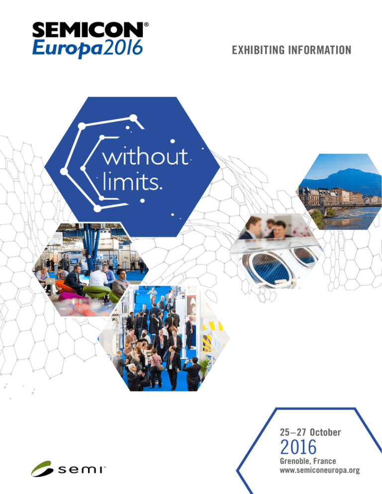
EXHIBITING INFORMATION
25 – 27 October
2016
Grenoble, France
www.semiconeuropa.org
SEMICON Europa 2016 in Grenoble: new opportunities in a
mature industry environment.
In 2016, SEMICON Europa will be back in Grenoble (France) following the long-term strategy for the
event, which rotates in alternate years between Grenoble (France) and Dresden (Germany), two of
Europe’s largest microelectronic clusters. With the support of public and private stakeholders across
Europe, the new SEMICON Europa strategy enables exhibitors to reach new audiences and business
partners and take full advantage of the strong microelectronic clusters in Europe.
Equipment spending for Europe positive in 2016
In Europe, Front End fab equipment spending is projected to increase 12.5 percent in 2015 (to US$
2.45 billion) and another 9.6 percent in 2016 (to $2.69 billion) according to most recent edition of the
SEMI World Fab Forecast (August 2015 edition).
Status as of September 2015, subject to change.
SEMICON Europa 2016
Book your exhibit space now and be part of SEMICON Europa 2016!
www.semiconeuropa.org
Welcome to Grenoble – Bienvenue à SEMICON Europa 2016!
INNOVATION FOR INDUSTRY
A dynamic economy linked to research
Leading national and international companies have come to the Grenoble area to benefit from
our scientific research. STMicroelectronics, IBM, Schneider Electric, France Telecom, Thales,
Hewlett Packard, Soitec, Teisseire, Vicat, Xerox, and others have all chosen Grenoble. The city’s
strong economy also stems from companies specialized in outdoor products such as the worldrenowned Petzl and Rossignol. Last but not least, more traditional industries branching out to
chemistry, heavy manufacturing, timber and paper, still have a prominent role to play, thanks
to companies such as Caterpillar, Alstom Hydro Power, Pomagalski and A. Raymond.
A scientific hub unlike any other in the world with:
• 3,600 researching professors in 129 university laboratories
• 3,700 doctoral students, 45% of whom are foreigners
• 9 national research bodies: CNRS, CEA, IRSTEA, CEN, CRSSA, INRA, INRIA, INSERM, IRD
• 5 major international facilities: ESRF, ILL, EMBL, GHMFL, IRAM
• 14,000 visiting foreign scientists every year
• 3 competitive centers: Minalogic, Tenerrdis, Axelera
• The Minalogic cluster fosters research-led innovation in intelligent miniaturized products
and solutions for industry. Located in Grenoble, the cluster channels in a single physical
location a range of highly-specialized skills and resources from knowledge creation to the
development and production of intelligent miniaturized services for industry.
GRENOBLE WELCOMES THE WORLD
ALPEXPO is the place in Grenoble where SEMICON Europa 2016 will be hosted. Recently
revamped, the venue’s unique, elegant architecture truly sets it apart and pays tribute to the
vision of architect Jean Prouvé who initialy designed ALPEXPO for the 1968 Winter Olympics.
Two international airports:
• Lyon Saint-Exupéry Airport (1 hour from Grenoble)
• Geneva Airport (1 hour 45 min from Grenoble)
Arriving by train:
• Central train station ideally located in the city center
• 3 hours from Paris (on the high speed TGV train)
SEMICON Europa Programs – focus on current industry needs
The SEMICON Europa technology and business programs are addressing the critical issues and
challenges facing the microelectronics industries and provides the information, education, and
guidance that you need to move your innovations and products to market. The 2016 program will
include the following key focus areas.
SEMICONDUCTOR TECHNOLOGY
•20th Fab Managers Forum
• Next Generation Lithography
• Emerging Research Materials
• Secondary Equipment Session
• Metrology, Process Control, Automation and Software
• Workshop on Equipment Assessment and Equipment Performance
Improvements
• MEMUNITY Workshop
TEST AND PACKAGING
• Advanced Packaging Conference
• 18th European Manufacturing Test Conference (EMTC)
PLASTIC ELECTRONICS CONFERENCE
• Hybrid and Heterogeneous Integration
• OLEDs, Displays and Lighting
• Integrated Smart Systems
EXECUTIVE AND MARKET
• Executive Sessions and Reception
• SEMI Market Briefing
• European Semiconductor Cluster Activities
APPLICATION AND INNOVATION PROGRAMS
•
•
•
•
Imaging Conference
Low Power Conference
Power Electronics Conference
Innovation Village
- Silicon Innovation Forum
- Innovation Conference
TechARENA & TechLOUNGE
TechARENAs at SEMICON Europa are the place to hear about the latest
technology developments and breakthroughs in semiconductor manufacturing.
All exhibiting companies have the opportunity to present their latest products
and new technologies at the TechLOUNGE exhibitor presentation sessions.
Enhanced scope of SEMICON Europa is supported by strong initiatives
and leverages on current industry trends!
Microelectronics – the Enabler for Industry 4.0
The European micro- and nanoelectronics industries are an essential driver of the
implementation of Industry 4.0 – considered to be the 4th revolution of industrial
manufacturing. The continuous advancements of the current automation in production
towards a “smart fab of the future” will be a step-by-step model in the upcoming years. Promising
areas for the microelectronics industry within Industry 4.0 are MEMS including sensors and actors,
embedded systems on chip including special sensors, microcontrollers and high-tech storage memory,
power electronics, data transportation, energy harvesting, system integration, and IT-security.
SEMICONDUCTOR MANUFACTURING AND TECHNOLOGY
The Semiconductor Manufacturing and Technology segment is the core exhibition area of SEMICON Europa.
It is the dedicated platform for companies offering equipment, materials or services for semiconductor
manufacturing including wafer manufacturing, test and packaging.
EQUIPMENT
- Wafer processing
- Inspection and measurement
- Assembly and test
- MEMS and nanotechnology
- Flat panel display
- Organic, large area and printed electronics
MATERIALS
-Gases
- Chemicals and solids
-Fluids
- Mask making
-Process
-Substrate
- Assembly and test
- MEMS and
nanotechnology
- Flat panel display
- Organic, large area and
printed electronics
• COMPONENTS, PARTS AND ACCESSORIES
• SUB-SYSTEMS
• FACTORY MONITORING AND CONTROL SYSTEMS
• HVAC, TEMPERATURE, HUMIDITY, CONTAMINATION CONTROL
• MATERIAL HANDLING SYSTEMS
• COMMUNICATION SOFTWARE
• DESIGN SOFTWARE
• MANUFACTURING SOFTWARE
• SIMULATION, ANALYSIS AND MODELING SOFTWARE
• MANUFACTURING SERVICES AND CONSULTING
• DISTRIBUTORS AND LOGISTICS
• EDUCATIONAL AND RESEARCH INSTITUTIONS
• FINANCIAL AND PROFESSIONAL SERVICES
• SUPPORT PRODUCTS
INNOVATION VILLAGE
START-UP ZONE
CLUSTER PAVILIONS
SHOW AND DEMONSTRATOR AREA
POWER ELECTRONICS CONFERENCE
On a global level, the field of integrated power electronics system has enormous potential for sustainable
innovation. Power electronics systems are a key enabling technology, not only for the generation, distribution,
and storage of electrical energy (for example harvesting energy from renewable resources, or DC grids with
bidirectional energy flow) but also for making less electrical energy do more for the people who use it (for
example, electrical mobility: bikes, cars, busses, trains, and airplanes, or next generation industrial
drive technology: Industry 4.0). The change from large, centralized electrical energy generation
to distributed, renewable generation – made possible by power electronics equipment – requires
automated systems with intelligent hard- and software, which has been continually accompanied by
interdisciplinary cooperation with microelectronics and computer science.
SPEAKER EXCTRACT FROM 2015:
Aalborg University
ABB Switzerland Ltd
CALY Technologies
CEA
CREE
EXAGAN
Fraunhofer IISB
Infineon Technologies
NaMLab GmbH
SGS INSTITUT FRESENIUS GmbH
Topsil Semiconductor Materials A/S
VEECO Instruments
Yole Développement
STMicroelectronics
Technische Universität Dresden
Universitätsklinikum Carl Gustav
Carus
Fairchild Semiconductor
IMAGING CONFERENCE
Electronic imaging and applications are advancing nearly as fast as integrated circuits in terms of
performance and innovation. In less than a decade, smartphone cameras have grown from a “nice to have”
feature, to a “must-have” solution for social photographers. Meanwhile, advances made in imaging are
opening doors to new commercial and consumer applications, including automotive, healthcare, security
and entertainment. The Imaging Application segment will highlight leading companies and innovative
products in the market.
SPEAKER EXCTRACT FROM 2015:
aSpect Systems
Basler AG
CEA / Leti
Chronocam
CNES
Continental AG
e2v
Fastree3D SA
FLIR
FotoNation Ltd.
Harvest Imaging
Heptagon Advanced MicroOptics
ID Quantique
InVisage Technologies Inc.
ISAE
ISORG
Kalray
Luxexcel
Microsoft
ON Semiconductor
Panono GmbH
Parrot
Pelican Imaging Corp.
PerkinElmer
pmdtechnologies gmbh
Raytrix GmbH
Red Belt SA
STFC
STMicroelectronics
Teledyne DALSA Professional
Imaging
TowerJazz
TU Delft
Universita dell’Insubria
University of Eastern Finland
Yole Développement
LOW POWER CONFERENCE
Exciting new applications such as safety enhanced automotive, medical monitoring or next-generation wearable
smart equipments in a number of systems will be powered by energy scavenging technologies. Already today,
whatever it is to get the best battery autonomy or to fit within the power budget, energy efficiency has
become a key challenge across most of applications. The winning approach will surely be to take the best
of the technologies potential, from silicon process to architecture implementation.
SPEAKER EXCTRACT FROM 2015:
CEA Leti
CSEM
ETH Zurich
Fraunhofer IIS
Fraunhofer IKTS
Fraunhofer IPMS
GLOBALFOUNDRIES
Hager Security
Infineon Technologies AG
NaMLab Gmbh
SOITEC
STMicroelectronics
Technische Universität Dresden
TU Dresden
Yole Développement
VISITOR PROFILE
SEMICON Europa attracts a highly influential audience from every segment and
sector of the European microelectronics industries, including semiconductors,
LEDs, MEMS, printed/organic/flexible, and other adjacent markets.
EXHIBITOR PROFILE
SEMICON EUROPA POST-SHOW DATA
MARKETS REPRESENTED
•Semiconductors
• LEDs / Solid State Lighting
•MEMS
• Printed / Organic Electronics
•Nano-Electronics
• Flat Panel Display (FPD)
• Photovoltaics / PV
23%
36%
32%
34%
Purchasing
Authority
Job
Levels
27%
13%
14%
23%
36%
14%
27%
7%
14%
Final Decision Maker
Recommend / Evaluate / Consult
Other Management
No Role
14%
13%
32%
34%
7%
Executive Management
Senior Management
Other Management
Staff Level/Professional
Other
KEY VISITING COMPANIES AND ORGANIZATIONS
SEMICON Europa attracts visitors from every major European microelectronics
company, including buying teams from leading IDMs, foundries, fabless, OSATs,
and OEMs.
TOP VISITING COMPANIES
ABB Semiconductors
ADEUNIS RF
AFELIM
AIRBUS
ALTIS
Altis Semiconductor
ams AG
ARM
Atmel Europe SARL
Becton Dickinson
CADENCE
CEA
CMOSIS
CNES, Toulouse
CNRS
Colibrys
Crocus Nano Electronics LLC
Dialog Semiconductor
e2v
Elmos Semiconductor AG
EM Microelectronic
EPCOS AG
Ericsson
Fab Owners Association
Fairchild Semiconductor
Fraunhofer EMFT
GLOBALFOUNDRIES
Hewlett Packard
Honeywell
Huawei
IMEC
Infineon
Intel
JSC Angstrem-T
Kalray
Lfoundry s.r.l.
Melexis
MEMC Electronic Materials
Micrel Semiconductor
Micron Semiconductor Italia
MICRONAS
Microoled
NXP
Okmetic
ON Semiconductor
Osram
Philips Innovation services
Plansee SE
Qualcomm Technologies
Robert Bosch GmbH
Safran Colibrys
SAMSUNG ELECTRONICS
Sensirion AG
Silex Microsystems AB
Sofradir
SOITEC
STMicroelectornics
TELEFUNKEN Semiconductors
Texas Instruments
Thales
Total
TriQuint Semiconductor
Trixell
Tronics
VISHAY
X-FAB MEMS Foundry
and more...
Partial list and data; see the SEMICON Europa 2014 Post-Show Report online at w
ww.semiconeuropa.org
for additional details and information.
SEMICON Europa exhibitors are the
suppliers to and partners of Europe’s
leading microelectronics companies.
SAMPLE PRODUCT CATEGORIES
MANUFACTURING EQUIPMENT
• Front-End Manufacturing Equipment
• Thin Film Manufacturing Equipment
• Test Equipment
• Assembly and Packaging Equipment
• Inspection and Measurement /
Metrology
MATERIALS
• Wafers and Substrates
• Process Materials
• Chemicals and Solids
•Gases
• Test Materials
• Assembly and Packaging Materials
SOFTWARE, OTHER PRODUCTS
AND SERVICES
•Sub-Systems
• Components Parts and Accessories
• Factory Control Automation /
Facilities
• Support Products (includes
consumables)
• Secondary Equipment and Services
• Software: Manufacturing / Factory
Automation
• Software: Electronic Design (EDA) /
Silicon Intellectual Property (IP)
• Manufacturing Services / Consulting
• Business Services / Consulting
EXHIBIT NOW!
CONTACT US TO RESERVE
YOUR BOOTH SPACE
BOOTH CONFIGURATION AND COSTS
RAW SPACE
Raw booth spaces are available as in-line, peninsula, and island configurations.
This option is the right solution for companies with custom exhibits. Raw space
covers floor rental only and does not include utilities, furnishings, labor or
other services.
RAW SPACE PRICE*
Booth space is allocated on a first come first served basis. Standard booths are
sold in increments of 9 square meters (3m x 3m).
• SEMI Member 295 EUR/sqm (+20% VAT for non-French companies)
• Non-Member 395 EUR/sqm (+20% VAT for non-French companies)
SEMI EUROPE OFFICE
Helmholtzstrasse 2-9
Building D / 3rd Floor
10587 Berlin, Germany
Sales Contact
Jerome Boutant
Tel: +33 6 09 46 62 75
Email: jboutant@semi.org
Operations Contact
Eva Weller
Tel: +49 30 3030 8077 11
Email: eweller@semi.org
SEMI GLOBAL HEADQUARTERS
Global Sales
Tel: +1 877 746 7788
+1 408 943 6901
Email: sales@semi.org
* Raw space is the rental of floor space only and does not include utilities, services, walls, carpet, furnishings,
labor, or material handling. Booths are sold in no less than 9 square meter increments unless otherwise
indicated on floor plan.
BOOTH PACKAGES
These booth packages are designed for exhibitors looking for a one-stop solution
that includes hardwall construction, floor space rental, furnishings, labor,
utilities, and other services.
For detailed pricing and exhibit options, please visit:
www.semiconeuropa.org
ABOUT SEMI
SEMI is the global industry association serving the manufacturing supply
chain for the micro- and nano-electronics industries, including semiconductors,
photovoltaics, LED, plastic/printed/organic electronics, MEMS, flat panel display
(FPD), and related markets.
For more than 40 years, SEMI has served its members and the industries it
represents through programs, initiatives, and actions designed to advance
business and market growth worldwide. SEMI supports its members through
a global network of offices, activities, and events in every major electronics
manufacturing region around the world.
www.semiconeuropa.org
25 – 27 October • Grenoble, France
Copyright © 2015. Semiconductor Equipment and Materials International (SEMI). All rights reserved.
SEMI and semi.org are trademarks or registered trademarks of SEMI in the United States and other
countries. All other company and product names are trademarks of their respective holders.
