Laser driver
advertisement

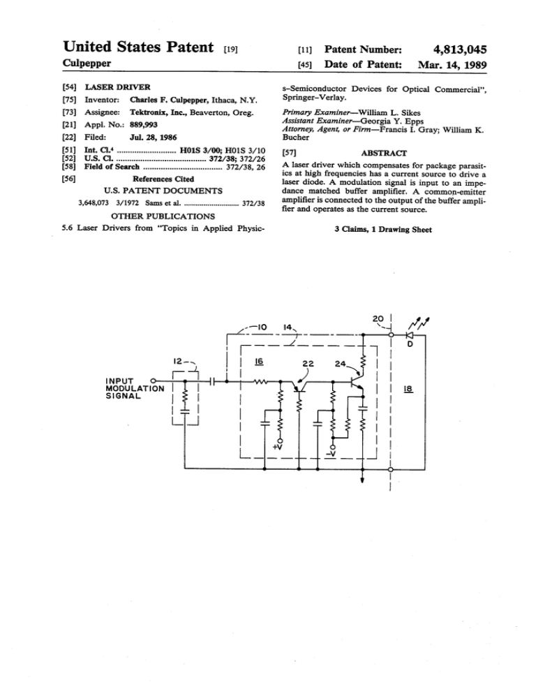
United States Patent [191 [11] [45] Culpepper [54] LASER DRIVER [75] Inventor: Charles F. Culpepper, Ithaca, NY. [73] Assignee: Tektronix, Inc., Beaverton, Oreg. [21] Appl. No.: 889,993 [22] Filed: Jul. 28, 1986 [51] [52] [58] Int. Cl.‘ ......................... .. H018 3/00; HOlS 3/10 US. Cl. ............................... .. 372/38; 372/26 Field of Search .................................. .. 372/38, 26 [56] References Cited U.S. PATENT DOCUMENTS 3,648,073 3/ 1972 Sams et al. .......................... .. 372/38 Patent Number: Date of Patent: 4,813,045 Mar. 14, 1989 s-Semiconductor Devices for Optical Commercial”, Springer-Verlay. Primary Examiner-William L. Sikes Assistant Examiner—Georgia Y. Epps Attorney, Agent, or Firm-Francis I. Gray; William K. Bucher [57] ABSTRACT A laser driver which compensates for package parasit ics at high frequencies has a current source to drive a laser diode. A modulation signal is input to an impe dance matched buffer ampli?er. A common-emitter ampli?er is connected to the output of the buffer ampli ?er and operates as the current source. OTHER PUBLICATIONS 5.6 Laser Drivers from ‘Topics in Applied Physic INPUT MODULATION SIGNAL 3 Claims, 1 Drawing Sheet 1 4,813,045 2 the laser diode D with concomitant degradation in per formance. As shown in FIG. 2 an input modulation signal is LASER DRIVER applied to an input RC impedance matching circuit 12 BACKGROUND OF THE INVENTION The present invention relates to laser drivers, and more particularly to a laser driver which allows high frequency continuous-wave modulation of laser diodes in the presence of package reactance. Currently laser diodes are driven from a ?fty (50) ohm source via a matching impedance transmission line which is AC coupled directly to the laser. The laser diode is enclosed in an hermetic package which in turn is mounted on a circuit board. At high frequencies the package parasitics due to the bond wires which connect the package to the circuit board tend to degrade the peformance of the laser diode since the bond wires tend emitter ampli?er 24 is connected to the laser diode D to provide the drive current. Also, as is well known in the to act as a series LC circuit. art, emitter degeneration of the common-emitter ampli What is desired is a laser drive circuit which compen sates for the package parasitics to minimize laser diode ?er 24 and interstage coupling between the buffer am pli?er 22 and the common-emitter ampli?er can be changed to ?atten response. The quiescent point of the and AC coupled to the laser driver circuit 14 which is located on a circuit board 16. The laser diode D is situ ated in a package 18 and connected to the circuit board via bond wires. The bond wire interface between the circuit board 16 and the package 18 is indicated by a dotted line 20. The laser driver circuit 14 has an input common-base buffer ampli?er 2 to which the input modulation signal is applied at the emitter. The collec tor of the buffer ampli?er 22 is input to the base of a common-emitter ampli?er 24 which is biased to operate in a current source mode. The collector of the common degradation at high frequencies. laser diode D is determined by another stage (not shown) connected to the laser diode through a low pass SUMMARY OF THE INVENTION Accordingly the present invention provides a laser ?lter, as is well known in the art. driver which allows high-frequency continuous-wave 25 Since the current to the laser diode D is derived from modulation of laser diodes in the presence of package the common-emitter ampli?er 24 operating as a current reactance with a minimum of degradation. The modula source, the effect of the reactance L is minimized as, tion signal is input via a common-base buffer ampli?er regardless of frequency, the laser diode is driven by a to a common-emitter ampli?er operating in a current source mode and having an essentially constant ampli constant amplitude a.c. component of the drive current. Thus the voltage divider effect of the reactance L is essentially eliminated, and the performance of the laser tude a.c. component. The current from the current source drives the laser diode. diode D is not degraded. Therefore, the present invention provides a laser The objects, advantages and novel features of the driver which uses a current source with an essentially present invention will be apparent from the following detailed description when read in conjunction with the 35 constant amplitude a.c. component to drive a laser diode in order to eliminate package parasitics due to appended claims and attached drawing. bond wire reactance at high frequencies. What is claimed is: BRIEF DESCRIPTION OF THE DRAWING FIG. 1 is an equivalent schematic view of a laser 1. A laser driver for a laser diode comprising: an impedance matched input buffer ampli?er to which ‘a modulation signal is applied; and diode with associated package parasitics. FIG. 2 is a schematic view of a laser driver according to the present invention. a current source coupled to the output of the impe dance matched input buffer ampli?er, the output of DESCRIPTION OF THE PREFERRED EMBODIMENT the current source providing an essentially con stant amplitude a.c. current component coupled to drive the laser diode. 2. A laser driver as recited in claim 1 wherein the Referring now to FIG. 1 an equivalent circuit for a laser diode D is shown. The laser diode is equivalent to impedance matched input buffer ampli?er comprises: a parallel combination of a resistor R and a capacitor C. In series with the laser diode D is shown a series induc an input impedance matching circuit to which the modulation signal is applied; and tance L which represents the reactance of the bond a common-base ampli?er with the emitter coupled to wires connecting the laser diode package to a circuit the input impedance matching circuit to receive board. As is apparent, if a conventional voltage driven, the modulation signal. direct drive circuit is used to modulate the laser diode 3. A laser driver as recited in claim 2 wherein the D, as indicated by the intermittent dotted line 10 in 55 current source comprises a common-emitter ampli?er FIG. 2, the reactance L created by the bond wires acts coupled to the collector of the common-base ampli?er, as a voltage divider with the laser diode. Since the the common-emitter ampli?er having its collector cou reactance L is directly related to frequency, at high pled to the laser diode to provide the essentially con frequencies more of the drive voltage appears across the stant amplitude a.c. drive current. i t t * t reactance, resulting in reduction of the drive current to 65


