Product Specification
PE45450
UltraCMOS® Power Limiter
9 kHz–6 GHz
Product Description
The PE45450 is a HaRP™ technology-enhanced power
limiter designed for use in high performance power
limiting applications in test and measurement equipment,
radar, military electronic counter measure receivers and
wireless infrastructure transceivers and antennas.
Unlike traditional PIN diode solutions, the PE45450
achieves an adjustable input 1 dB compression point or
limiting threshold via a low current control voltage (VCTRL),
eliminating the need for external bias components, such
as DC blocking capacitors, RF choke inductors, and bias
resistors.
It delivers low insertion loss and high linearity under nonlimiting input power levels and extremely fast response
and recovery time in a limiting event. It also offers
superior ESD rating and ESD protection for subsequent
circuitry.
The PE45450 is manufactured on Peregrine’s
UltraCMOS® process, a patented variation of silicon-oninsulator (SOI) technology on a sapphire substrate.
Peregrine’s HaRP™ technology enhancements deliver
high linearity and excellent harmonics performance. It is
an innovative feature of the UltraCMOS process, offering
the performance of GaAs with the economy and
integration of conventional CMOS.
Features
Monolithic drop-in solution with no
external bias components reducing
design complexity
Adjustable power limiting threshold
from +25 dBm to +35 dBm
Max power handling
+40 dBm CW (10W)
+47 dBm Pulsed (50W)
Superior ESD rating and ESD protection
8 kV HBM on all pins
1 kV CDM on all pins
600V MM on all pins
Unbiased power limiting operation
Fast response and recovery time of 1 ns
Dual mode operation
Power limiting mode
Power reflecting mode
Figure 2. Package Type
12-lead 3x3 mm QFN
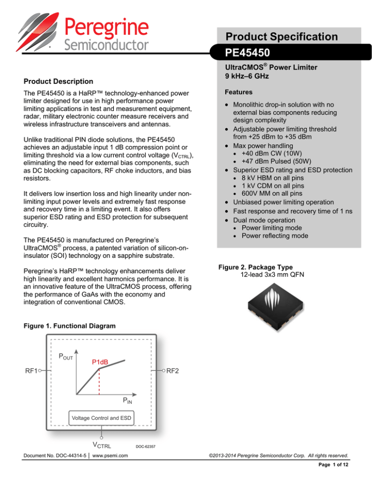
Figure 1. Functional Diagram
POUT
P1dB
RF1
RF2
PIN
Voltage Control and ESD
VCTRL
Document No. DOC-44314-5 │ www.psemi.com
DOC-62357
©2013-2014 Peregrine Semiconductor Corp. All rights reserved.
Page 1 of 12
PE45450
Product Specification
Table 1. Electrical Specifications @ +25°C (ZS = ZL = 50Ω), unless otherwise noted
Parameter
Condition
Operating frequency
Min
Typ
9 kHz
Max
Unit
6 GHz
As shown
0.70
1.05
dB
dB
Power limiting mode
Insertion loss1
9 kHz–3 GHz
3–6 GHz
0.45
0.80
Return loss1
9 kHz–3 GHz
3–6 GHz
13
17
dB
dB
P1dB / limiting threshold
VCTRL = –2.5V @ 915 MHz
VCTRL = –1.5V @ 915 MHz
VCTRL = –0.5V @ 915 MHz
35
32
25
dBm
dBm
dBm
Leakage power2
VCTRL = –2.5V @ 915 MHz
VCTRL = –1.5V @ 915 MHz
VCTRL = –0.5V @ 915 MHz
33.5
33
31.5
VCTRL = –1.0V @ 915 MHz
0.4
VCTRL = 0V @ 915 MHz
25
Input IP2
VCTRL = –2.5V @ 915 MHz
VCTRL = –2.5V @ 6 GHz
115
110
dBm
dBm
Input IP3
VCTRL = –2.5V @ 915 MHz
VCTRL = –2.5V @ 6 GHz
70
60
dBm
dBm
1 GHz
1
ns
Leakage power2
VCTRL = +2.5V @ 915 MHz
2
Switching time4
State change to 10% RF
Leakage power slope
Unbiased leakage power
2
Response / recovery time
Power reflecting mode
Notes:
35.5
35
33.5
dBm
dBm
dBm
dB/dB
27
dBm
3
400
8
dBm
µs
1. External matching is required to achieve the performance.
2. Measured with +40 dBm CW applied at input.
3. This mode requires the control voltage to toggle between +2.5V and –2.5V. At +2.5V, the limiter equivalent
circuit is a low impedance to ground, reflecting most of the incident power back to the source.
4. State change is VCTRL toggle from –2.5V to +2.5V.
©2013-2014 Peregrine Semiconductor Corp. All rights reserved.
Page 2 of 12
Document No. DOC-44314-5 │ UltraCMOS® RFIC Solutions
PE45450
Product Specification
Figure 3. Pin Configuration (Top View)*
Table 3. Operating Ranges
Parameter
Control voltage
Power limiting mode
Power reflecting mode
RF input power, CW1
RF input power, pulsed
2
RF input power, unbiased2,3
Operating temperature
range
Operating junction
temperature1
Notes:
Symbol
Min
VCTRL
–2.5
–2.5
Typ
Max Unit
–0.5
+2.5
V
V
PMAX,CW
40
dBm
PMAX,PULSED
47
dBm
PMAX,UNB
47
dBm
+85
°C
+290
°C
TOP
–55
+25
TJ
1. CW, 100% duty cycle, in 10 min, 50Ω
2. Pulsed, 0.1% duty cycle of 1 µs pulse width in 10 min, 50Ω
3. VCTRL = 0V or VCTRL pin left not connected
Table 4. Absolute Maximum Ratings
Note: * Pins 10–12 can be ground if deemed necessary by the customer.
Symbol
Min
Max
Unit
Control voltage
Power limiting mode
Power reflecting mode
VCTRL
–3.3
3.6
V
Storage temperature range
TST
–65
+150
°C
VESD,HBM
8000
V
VESD,MM
600
V
VESD,CDM
1000
V
Parameter
Table 2. Pin Descriptions
Pin No.
Pin Name
1, 3, 4, 6,
7, 9
GND
2
RF1*
Description
Ground
RF port 1
1
ESD voltage HBM , all pins
2
ESD voltage MM , all pins
3
5
VCTRL
Control voltage
ESD voltage CDM , all pins
8
RF2*
RF port 2
Notes:
10–12
N/C
No connect
Pad
GND
Exposed pad: Ground for proper operation
Note: * RF pins 2 and 8 must be at 0 VDC. The RF pins do not require DC
blocking capacitors for proper operation if the 0 VDC requirement is met.
Latch-Up Avoidance
Unlike conventional CMOS devices, UltraCMOS
devices are immune to latch-up.
Moisture Sensitivity Level
The Moisture Sensitivity Level rating for the
PE45450 in the 12-lead 3x3 mm QFN package is
MSL1.
Document No. DOC-44314-5 │ www.psemi.com
1. Human Body Model (HBM, MIL_STD 883 Method 3015.7)
2. Machine Model (JEDEC JESD22-A115)
3. Charged Device Model (JEDEC JESD22-C101)
Exceeding absolute maximum ratings may cause
permanent damage. Operation should be
restricted to the limits in the Operating Ranges
table. Operation between operating range
maximum and absolute maximum for extended
periods may reduce reliability.
Electrostatic Discharge (ESD) Precautions
When handling this UltraCMOS device, observe
the same precautions that you would use with
other ESD-sensitive devices. Although this device
contains circuitry to protect it from damage due to
ESD, precautions should be taken to avoid
exceeding the rating specified.
©2013-2014 Peregrine Semiconductor Corp. All rights reserved.
Page 3 of 12
PE45450
Product Specification
ESD Protection Capability
Dual Mode Operation
The PE45450 can be used as an ESD protection
device to protect sensitive circuit elements against
ESD surges. Besides superior ESD rating of 8 kV
HBM, the PE45450 has excellent voltage
clamping capability. During an ESD event, the
PE45450 maintains very low voltage across the
device to ensure that the circuit element it is
protecting survives.
Power Limiting Mode
The PE45450 performs as a linear power limiter
with adjustable P1dB / limiting threshold. The
P1dB / limiting threshold can be adjusted by
changing the control voltage between –2.5V and
–0.5V. If unbiased, or if VCTRL = 0V, the PE45450
still offers power limiting protection.
Power Reflecting Mode
Power reflecting mode requires a power detector
to sample the RF input power and a
microcontroller to toggle the limiter control voltage
between +2.5V and –2.5V based on the system
protection requirements. At +2.5V, the limiter
impedance to ground is less than 1Ω and most of
the incident power will be reflected back to the
source. At –2.5V, the device operates as in
power limiting mode.
Table 5. Transmission Line Pulse Data vs. HBM
VCTRL
HBM (V)
Max Current (A)
Voltage (V)
0
1000
0.7
3.7
–1.5
1000
0.7
18
0
2000
1.3
7
–1.5
2000
1.3
20
0
3000
2.0
10.8
–1.5
3000
2.0
21.5
Figure 4. Transmission Line Pulse Curve
10
9
8
7
Current(A)
6
5
4
Vctrl=0V
3
Vctrl=‐1.5V
2
1
0
0
5
10
15
20
25
30
Voltage(V)
©2013-2014 Peregrine Semiconductor Corp. All rights reserved.
Page 4 of 12
Document No. DOC-44314-5 │ UltraCMOS® RFIC Solutions
PE45450
Product Specification
Thermal Data
When limiting high power RF signals, the junction
temperature of the power limiter can rise
significantly.
Table 6. Theta JC
Parameter
Theta JC
Min
Typ
20
Max
Unit
°C/W
Special consideration needs to be made in the
design of the PCB to properly dissipate the heat
away from the part and maintain the 290°C peak
junction temperature.
It is recommended to use best design practices for
high power QFN packages: multi-layer PCBs with
thermal vias in a thermal pad soldered to the slug
of the package. Special care also needs to be
made to alleviate solder voiding under the part.
Document No. DOC-44314-5 │ www.psemi.com
©2013-2014 Peregrine Semiconductor Corp. All rights reserved.
Page 5 of 12
PE45450
Product Specification
Typical Performance Data @ +25°C, 915 MHz (ZS = ZL = 50Ω), unless otherwise noted
Figure 5. Insertion Loss vs. Temperature
Figure 6. Input Return Loss vs. Temperature
©2013-2014 Peregrine Semiconductor Corp. All rights reserved.
Page 6 of 12
Figure 7. Output Return Loss vs. Temperature
Document No. DOC-44314-5 │ UltraCMOS® RFIC Solutions
PE45450
Product Specification
Typical Performance Data @ +25°C, 915 MHz (ZS = ZL = 50Ω), unless otherwise noted
Figure 8. POUT vs. PIN Over VCTRL
–1.5V
–0.7V
–0.5V
0V
2.5V
–0.7V @ 915 MHz
40
40
35
35
30
30
25
25
Pout (dBm)
Pout (dBm)
–2.5V
Figure 9. POUT vs. PIN Over Frequency @
VCTRL = –0.7V
20
15
–0.7V @ 3 GHz
–0.7V @ 6 GHz
20
15
10
10
5
5
0
0
10
15
20
25
Pin (dBm)
30
35
40
Figure 10. P1dB vs. VCTRL Over Temperature
P1dB @ –55°C (dBm)
P1dB @ 25°C (dBm)
10
15
20
25
Pin (dBm)
30
35
40
Figure 11. POUT vs. PIN Over Frequency @
VCTRL = –1.5V
P1dB @ 85°C (dBm)
–1.5V @ 915 MHz
40
–1.5V @ 3 GHz
–1.5V @ 6 GHz
40
35
35
30
Pout (dBm)
P1dB (dBm)
30
25
25
20
15
10
20
5
15
‐2.5
‐2
‐1.5
VCTRL (V)
Document No. DOC-44314-5 │ www.psemi.com
‐1
‐0.5
0
10
15
20
25
Pin (dBm)
30
35
40
©2013-2014 Peregrine Semiconductor Corp. All rights reserved.
Page 7 of 12
PE45450
Product Specification
Typical Performance Data @ +25°C, 915 MHz (ZS = ZL = 50Ω), unless otherwise noted
Figure 12. IIP3 / IIP2 vs. VCTRL Over Temperature
Figure 13. IIP3 / IIP2 vs. PIN Over VCTRL
IIP3 @ –55°C (dBm)
IIP3 @ 25°C (dBm)
IIP3 @ 85°C (dBm)
IIP3 @ VCTRL = –2.5V (dBm)
IIP2 @ VCTRL = –2.5V (dBm)
IIP3 @ VCTRL = –1.5V (dBm)
IIP2 @ –55°C (dBm)
IIP2 @ 25°C (dBm)
IIP2 @ 85°C (dBm)
IIP2 @ VCTRL = –1.5V (dBm)
IIP3 @ VCTRL = –0.7V (dBm)
IIP2 @ VCTRL = –0.7V (dBm)
IIP3 @ VCTRL = –0.5V (dBm)
IIP2 @ VCTRL = –0.5V (dBm)
130
120
100
IIP3 / IIP2 (dBm)
90
80
70
60
50
40
30
‐2.5
‐2
‐1.5
VCTRL (V)
‐1
‐0.5
10
20
25
30
35
Figure 15. P1dB, IIP3, IIP2, Leakage Power @
PMAX vs. VCTRL
IIP3 (dBm)
Leakage Power (25°C) @ Pmax
IIP2 (dBm)
P1dB (dBm)
Leakage Power @ Pmax
120
38
110
36
100
34
90
32
80
30
70
28
60
26
50
24
40
22
‐5
30
20
‐10
20
Leakage Power (85°C) @ Pmax
40
35
IIP3 / IIP2 / P1 dB (dBm)
30
Leakage Power (dBm)
15
Pin (dBm)
Figure 14. Leakage Power @ PMAX vs. VCTRL
Over Temperature
Leakage Power (–55°C) @ Pmax 140
130
120
110
100
90
80
70
60
50
40
30
20
25
20
15
10
5
0
‐2.5
‐2
‐1.5
‐1
‐0.5
0
0.5
1
1.5
2
VCTRL (V)
©2013-2014 Peregrine Semiconductor Corp. All rights reserved.
Page 8 of 12
2.5
Leakage Power @ Pmax (dBm)
IIP3 / IIP2 (dBm)
110
18
‐2.5
‐2
‐1.5
VCTRL (V)
‐1
‐0.5
Document No. DOC-44314-5 │ UltraCMOS® RFIC Solutions
PE45450
Product Specification
Evaluation Kit
Figure 16. Evaluation Board Layout
The power limiter EVK board was designed to
ease customer evaluation of Peregrine’s
PE45450. The bi-directional RF input and
output are connected to RF1 and RF2 port
through a 50Ω transmission line via SMA
connectors J2 and J3. A through 50Ω
transmission line is available via SMA
connectors J5 and J6. This transmission line
can be used to estimate the loss of the PCB
over the environmental conditions being
evaluated. The 2-pin connector J4 is
connected to the external bias VCTRL.
The board is constructed of a four metal layer
material with a total thickness of 62 mils. The
top RF layer is Rogers RO4350B material with
a 6.6 mil RF core and Er = 3.66. The middle
layers provide ground for the transmission
lines. The transmission lines were designed
using a coplanar waveguide with ground plane
model using a trace width of 13.5 mils, trace
gaps of 10 mils, and metal thickness of
2.1 mils.
Document No. DOC-44314-5 │ www.psemi.com
PRT-51452
©2013-2014 Peregrine Semiconductor Corp. All rights reserved.
Page 9 of 12
PE45450
Product Specification
Figure 17. Evaluation Board Schematic
NOT USED FOR PE45450
VDD
J1
1 1
2 2
R1
DNI
DNI
C3
50 OHM
1 GND
2 RF1
3 GND
C1
0.3pF
PE45450
50 OHM
GND 9
RF2 8
GND 7
13 DAP
J2
4 GND
5 VCTRL
6 GND
U1
N/C 12
N/C 11
N/C 10
DNI
C2
0.3pF
J3
J5
50 OHM
J6
THRU
C4
DNI
R2
0 Ohm
J4
1 1
2 2
HEADER2
Caution: Contains parts and assemblies susceptible to damage by electrostatic discharge (ESD).
©2013-2014 Peregrine Semiconductor Corp. All rights reserved.
Page 10 of 12
DOC-44327
Document No. DOC-44314-5 │ UltraCMOS® RFIC Solutions
PE45450
Product Specification
Figure 18. Package Drawing
12-lead 3x3 mm QFN
A
0.30
(x12)
0.10 C
(2X)
3.00
0.50
1.80±0.10
B
0.30±0.05
(x12)
(x8)
0.70
(x12)
0.50
(x8)
3.00
1.80±0.10
1.90
3.10
0.25±0.05
(x12)
0.10 C
1.00
Ref.
(2X)
PIN #1 CORNER
TOP VIEW
1.90
3.80
BOTTOM VIEW
0.10
0.05
0.10 C
0.50±0.05
0.05 C
RECOMMENDED LAND PATTERN
DOC-52193
C A B
C
ALL FEATURES
SEATING PLANE
SIDE VIEW
0.152
Ref.
0.02
C
Figure 19. Top Marking Specifications
45450
YYWW
ZZZZZZ
= Pin 1 designator
45450 = Five digit part number
YYWW = Date Code, last two digits of the year and work week
ZZZZZZ = Maximum six characters of the assembly lot code
DOC-51207
Document No. DOC-44314-5 │ www.psemi.com
©2013-2014 Peregrine Semiconductor Corp. All rights reserved.
Page 11 of 12
PE45450
Product Specification
Figure 20. Tape and Reel Drawing
Table 7. Ordering Information
Order Code
Description
Package
Shipping Method
PE45450A-X
PE45450 Power limiter
Green 12-lead 3x3 mm QFN
500 units / T&R
EK45450-02
PE45450 Evaluation kit
Evaluation kit
1 / box
Sales Contact and Information
For sales and contact information please visit www.psemi.com.
Advance Information: The product is in a formative or design stage. The datasheet contains design target
specifications for product development. Specifications and features may change in any manner without notice.
Preliminary Specification: The datasheet contains preliminary data. Additional data may be added at a later
date. Peregrine reserves the right to change specifications at any time without notice in order to supply the best
possible product. Product Specification: The datasheet contains final data. In the event Peregrine decides to
change the specifications, Peregrine will notify customers of the intended changes by issuing a CNF (Customer
Notification Form).
The information in this datasheet is believed to be reliable. However, Peregrine assumes no liability for the use
of this information. Use shall be entirely at the user’s own risk.
©2013-2014 Peregrine Semiconductor Corp. All rights reserved.
Page 12 of 12
No patent rights or licenses to any circuits described in this datasheet are implied or granted to any third party.
Peregrine’s products are not designed or intended for use in devices or systems intended for surgical implant,
or in other applications intended to support or sustain life, or in any application in which the failure of the
Peregrine product could create a situation in which personal injury or death might occur. Peregrine assumes no
liability for damages, including consequential or incidental damages, arising out of the use of its products in
such applications.
The Peregrine name, logo, UltraCMOS and UTSi are registered trademarks and HaRP, MultiSwitch and DuNE
are trademarks of Peregrine Semiconductor Corp. Peregrine products are protected under one or more of
the following U.S. Patents: http://patents.psemi.com.
Document No. DOC-44314-5 │ UltraCMOS® RFIC Solutions
