`Tlc`il.
advertisement

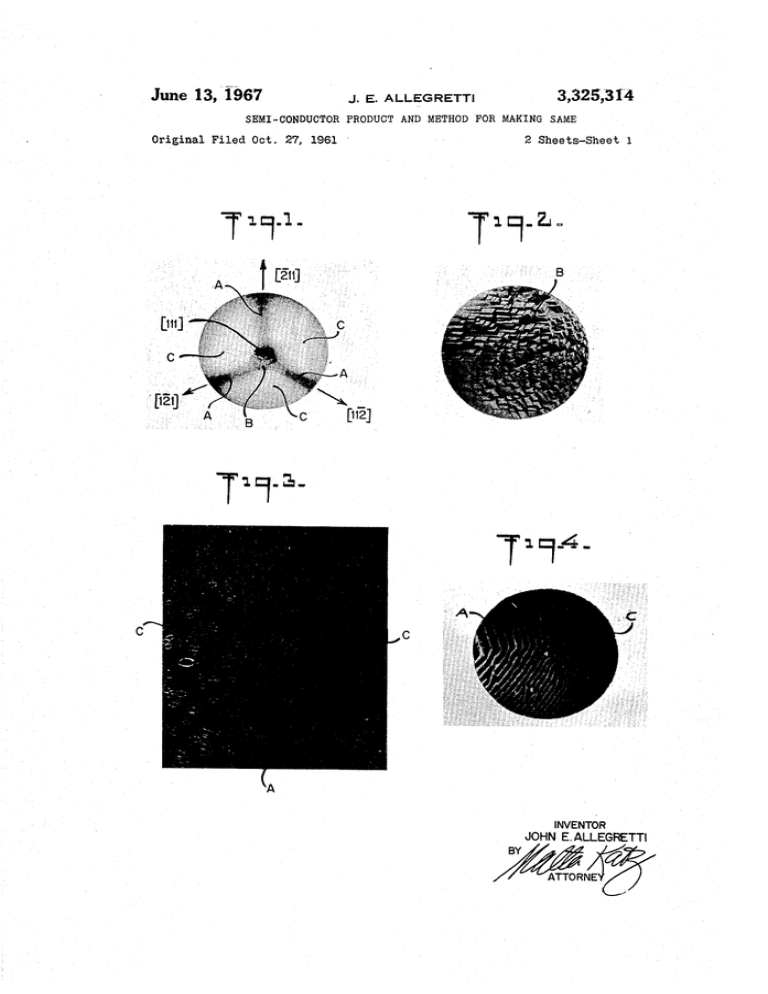
June 13,'i“967 J, E. ALLEF'GRETTI 3,325,314 SEMI-CONDUCTOR PRODUCT AND METHOD FOR MAKING SAME Original Filed Oct. 27, 1961 ‘ ' 2 Sheets-Sheet 1 'Tlc’il. INVENTCSR JOHN E.ALLEGRETTI W 4/ ATTORNE June 13, 1967 J. E. ALLEGRETTI 3,325,314 SEMI-CONDUCTOR PRODUCT AND METHOD FOR MAKING SAME Original Filed Oct. 2'7, 1961 2 Sheets-Sheet 2 INVENTOR JOH E. ALLEGRETTI United States Patent 0 1 ICC I Patented June 13, 1967 1 2 strates in accordance with the invention starting with a 3,325,314 single crystal of semiconductor material. SEMI-CONDUCTOR PRODUCT AND MUETHOD FOR MAKING SAME In accordance with the present invention there is pro vided a single crystal silicon semiconductor body includ ing a plurality of layers of single crystal ‘semiconductor John E. Allegrctti, East Brunswick, NJ, assignor to Sie mens & Halslre Aktiengesellschaft, Berlin and Munich, Germany, a corporation of Germany Continuation of application Ser. No. 148,253, Oct. 27, material, and wherein the surface layer of the body has a substantially improved surface quality. The semiconduc 1961. This application Aug. 27, 1965, Ser. No. 497,581 4 Claims. (Cl. l48--1'75) tor bodies produced herein have surfaces which are ex 10 This invention is a continuation of my copending ap plication Ser. No. 148,253 ?led Oct. 27, 1961, now aban doned, and relates to single crystal silicon semiconductor bodies grown from the vapor phase by thermal decom position and, more particularly, it relates to a method of growth of silicon semiconductor layers having a ?at, im onto a single crystal silicon semiconductor substrate which is oriented in a preferred manner. In particular, in the present invention, a silicon substrate is oriented at least three-eighths of a degree and not more than ?ve degrees off orientation from a low order Miller Indices growth plane. In a speci?c embodiment of the invention, The process of deposition of silicon semiconductor ma simultaneous thermal decomposition of a silicon com pound and active impurity compounds therewith in the presence of hydrogen is well known in the art. What is found is that thermal decomposition of silicon under these conditions produces surfaces with one or more ceedingly ?at and imperfection-free. In a preferred form of the present invention, single crystal semiconductor bodies having such improved surface qualities are pre pared by thermal decomposition from the vapor phase perfection-free surface. terial and active impurities therewith onto a single crystal silicon semiconductor substrate from the vapor phase by 3,325,314 silicon semiconductor bodies having ?at, imperfection free surfaces are produced by orienting the substrate in the aforementioned predetermined amount off orientation in the [111] plane of the crystal along a [211]<211> direction. As another feature of the present invention there is 25 provided a method of making such silicon semiconductor surface imperfections. For example, the surface may ex bodies having these improved surface qualities by growth hibit pyramidal growth, both rectangular and triangular in shape. Other imperfections manifest themselves in the form of pitting and growth stops wherein small hillocks from the vapor phase. In accordance with this method, growth from the vapor phase is effected by thermal de composition of a semiconductor material and active im are present on the surface, or as thickness deformities 30 purities therewith in the presence of hydrogen onto ‘a which occur in the form of a coarse texture or shingle ap silicon semiconductor substrate oriented in a predeter pearance on the surface. As will be apparent to others mined manner at deposition temperatures in the range skilled in the art, the availability or vapor-grown, flat, im of 1150-1200° C. perfection-free, single crystal semiconductor surfaces The process of growth from the vapor phase employed would enable the fabrication of semiconductor devices of 35 in the formation of semiconductor bodies in accordance improved quality. with the invention utilizes known thermal semiconductor An object of this invention is to provide a single materials with the only criterion being that a decompos crystal silicon semiconductor body including a plurality of layers of single crystal silicon semiconductor mate “thermally decomposable,” “thermal decomposition” and rial of different conductivity separated by a transition region wherein said body has a ?at, imperfection-free the associated deposit of a product. of decomposition, as used herein, are intended to be generic to the mechanisms able vapor source of the material be available. The terms surface. of heat-cracking as, for example, the decomposition of Still another object of the instant invention is to provide silicochloroform or silicon tetrachloride and liberation of a single crystal silicon semiconductor body by growth silicon atoms through the mechanism of high temperature reactions wherein the high temperature causes interaction from the vapor phase having a surface layer which has a substantially improved surface quality, by growth onto a single crystal silicon semiconductor substrate having a between various materials with liberation of speci?c ma terials or atoms as, for example, the reaction of silico~ predetermined crystal orientation. chloroform and hydrogen: Among the other objects of the invention is to provide a method of making such bodies by thermal decomposi tion from the vapor phase. These and other objects will be made apparent from the following more detailed description of the invention, in used in the preferred embodiments of this invention as hereinafter indicated. Single crystalline silicon semiconductor bodies in ac cordance with the invention may he formed, in general, which reference will be made to the accompanying draw ings, in which: utilizing the apparatus and techniques described in the FIGURE 1 is a photolithographic reproduction of the teachings of patent application SN. 86,239 by Benzing, surface characteristics of a single crystal silicon semicon Krsek and Topas, ?led Jan. 31, 1961, and now Patent ductor layer formed by growth from the vapor phase; No. 3,131,098. As is disclosed in the Benzing et a1. ap and regions marked A illustrate the imperfection-free sur plication, semiconductor material is deposited upon a faces produced according to the present invention, where 60 heated essentially single crystal semiconductor starting as those designated as B and C are indicative of the char element from a decomposable source thereof in a reaction acteristics of surfaces produced in the prior art; chamber. After a predetermined period of time during which the desired thickness of semiconductor material has been deposited, the reaction chamber is ?ushed with FIGURE 2 is a more detailed view of region B; FIGURE 3 shows regions A and C under high mag 65 a gas to remove unwanted atoms of active impurity there ni?cation; FIGURE 4 is an interference pattern of regions A and C; from. Thereafter, additional semiconductor decompos ‘ FIGURE 5 is a schematic illustration, in section, of a silicon semiconductor substrate oriented in accordance with the present invention; and FIGURE 6 shows a manner of preparing oriented sub— 70 able source material and atoms of active impurity of a desired type and degree are introduced into the reaction chamber and an additional layer of desired thickness of semiconductor material is deposited in essentially single crystalline form contiguous with the layer of material pre 3,325,314 3 4 viously deposited. This process may be continued until single crystal ‘silicon semiconductor bodies having im such a time as the desired numbers of layers of semi proved surface qualities. In a preferred form of the in vention a silicon crystal substrate is provided which is conductor material of alternating conductivity type or degree, each having a junction separating it from the ad jacent layer, are formed. As is evident, any desired num ber of layers of material, and any desired number of junc oriented at least % of a degree and not more than ?ve UK tions, may be formed in accordance with any given design considerations. degrees off orientation from a [111] plane of the crystal in the <§11> direction. Then a layer of silicon is de posited thereon by thermally decomposing silicochloro form and hydrogen at 1l50—1200°C. The layer thus formed has a clear, flat and substantially imperfection Referring now to FIGURE 1, there is shown an actual photolithographic reproduction of the surface of a single 10 free surface and the same orientation as that of the sub crystal silicon layer formed by thermal decomposition strate. of silicochloroform and hydrogen at 1150-1200° C. onto While the invention has been described with particular a single crystal silicon substrate oriented in a predeter reference to the formation of an individual semiconductor mined manner. In particular, the substrate is formed by body having improved surface qualities, it will be under providing a 4° arc of curvature from a [111] plane of the 15 stood that a plurality of such bodies may be formed crystal, thereby exposing a number of crystal planes simultaneously. Within the temperature ranges speci?ed which are close to a [111] plane. In this manner, it is pos sible to illustrate in a single experiment the characteris herein, a plurality of such bodies may be formed without appreciable diffusion of impurities from one body to an tics of layers formed on different substrate crystal planes. other during the deposition process. As may be seen in the drawing, certain regions contain 20 I claim: surface imperfections characteristic of those surfaces pre 1. A method for epitaxial depositing monocrystalline viously obtained in the art. On the other hand, other silicon from the gaseous phase onto a heated substrate regions exhibit a surface which is substantially imperfec which comprises epitaxially vapor-depositing monocrys tion-free. It is the latter surfaces ‘which are characteristic talline silicon at least primarily on a ?at deposition sur of those produced according to the present invention and face which departs at least 3/8 of a degree and not more which are so dramatically to be distinguished from those than 5 degrees off orientation from a [111] plane of the produced in the past. crystal in the <§ll> direction. As may be observed, the region marked A in FIGURE 1 is essentially clear and free of any undesirable sur face imperfections. The regions marked B and C, how 2. A single crystal silicon semiconductor body com prising a substrate of single crystal silicon semiconductor ' ever, have one or more surface imperfections. Region B, material of predetermined conductivity oriented at least % of a degree and not more than 5 degrees off orienta for example, is illustrative of a pyramidal growth imper tion from a [111] plane of the crystal in the <§11> di fection. FIGURE 2 shows this type of growth in more detail. Region C contains a form of surface imperfection rection and a single crystal silicon semiconductor mate rial, of conductivity different from that of said substrate layer, vapor-deposited by thermal decomposition on said substrate layer, said vapor-deposited layers having a clear, ?at, substantially imperfection-free surface and having the called “hillock-tylpe” growth. FIGURE 3 shows region C under high magni?cation. In FIGURE 4 there is shown the interference pattern, characteristic of regions A and C, under optical examina same orientation as the substrate. tion. What is shown therein is that the surface layer in region A is substantially free of distorting interference 40 patterns, which indicates that the region is free of sur~ face imperfections. Stated in more mathematical terms, region A has less than one interference line across 20 mm. of the surface thereof. Region C, on the other hand, has very many such lines in the same length. 45 The desired type of surface quality exhibited in region A occurs on that portion of the silicon crystal which is oriented at least 3/8 of a degree and not more than 5° off 3. A single crystal silicon semiconductor body com prising a substrate of single crystal silicon semiconductor material of predetermined conductivity oriented at least 3/8 of a degree and not more than 5 degrees off orientation from a [111] plane of the crystal in the <§11> direction and a single crystal silicon semiconductor material, of conductivity different from that of said substrate layer, formed by thermal decomposition from the vapor phase on said substrate layer, said vapor-deposited layers hav ing a clear, ?at substantially imperfection-free surface characterized by having less than one interference line orientation from a [111] plane in the <211> direction of the crystal. Single crystal silicon semiconductor sub 50 per 20 mm. of length across said surface and havinghthe strates which are oriented in this manner, have on an same orientation as the substrate. atomic scale, a number of atoms of semiconductor ma terial arranged in the form of steps. This stepwise ar rangement exposes a large number of atomic layers of the material, as illustrated in FIGURE 5. In a given length of exposed surface there are a number of exposed 4. A single crystal silicon semiconductor body com prising a substrate of single crystal silicon semiconductor atomic layers, the exact number varying with the extent to which the crystal is oriented off from a low Miller in dices crystal plane. For example, if the silicon crystal is oriented % of a degree off orientation there are 1.42><105 atomic layers exposed per centimeter of length . of the crystal. At a preferred 1.5° off orientation from the [111] plane, there are 4.9x 10⁵ such exposed atomic lay material doped to one conductivity oriented at least % of a degree and not more than ?ve degrees off orientation from a low Miller indices plane, the highest Miller index not exceeding 2, and a single crystal silicon semiconductor material of conductivity different from that of said sub strate layer vapor-deposited by thermal decomposition on said substrate layer, said vapor-deposited layers having a clear, ?at, substantially imperfection-free surface and hav in gthe same orientation as the substrate. References Cited UNITED STATES PATENTS ers, and at 5° there are 1.9><106 exposed atomic layers. In order to achieve the desired imperfection-free growth it is 65 necessary that the number of exposed atomic layers be within the limits enumerated above. FIGURE 6 illustrates a manner of preparation of a suitably oriented silicon single crystal substrate 10 in 3,200,001 8/1965 Merkel et al _______ __ 23-2235 OTHER REFERENCES Ingham et al., article in Metallurgy of Elemental and accordance with the invention. A cut along the lines 11 70 Compound Semiconductors, volume 12, Metallurgical So— 12 is made in the single crystal body in the manner ciety Conference, Aug. 29—31, 1960, pages 285-299. shown at an angle 0, thereby exposing a surface 13. The HYLAND BIZOT, Primary Examiner. cut is made 0 degrees off [111] orientation in the <'2I11> DAVID L. RECK, Examiner. direction of the crystal. . What has been described is a method for producing 75 N. F. MARKVA, Assistant Examiner.


