®
RT9186A/B
Low Profile 500mA LDO with Enable and Power Good/Reset
General Description
Features
The RT9186 is a low-dropout linear regulator providing up
to 500mA load current with 160mV dropout. It is especially
designed for the application of portable and smart handheld
device.
2.5V to 5.5V Wide Input Range
Guaranteed 500mA Output Current
Low 160mV Dropout at 500mA
1.8V/2.5V/3.3V Preset Output Voltage Version with
Adjustable Range from 0.8V to 4.5V.
Reset Output with 6ms (typ.) Delay Time
Power Good Output
Low 190μ
μA Ground Pin Current
0.1μ
μA Shutdown Current
Thermal and Over Current Protection
RoHS Compliant and 100% Lead (Pb)-Free
The RT9186 operates from 2.5V to 5.5V supply. The
internal P-MOSFET pass transistor allows the regulator
to work with 190μA low quiescent current. Its preset output
voltage version covers the most frequently used values,
including 1.8V/2.5V/3.3V. Output voltage can also be
adjusted via the ADJ pin for those other than the preset
values.
With only 0.1μA required in the shut down mode, one
enable pin is able to control output on/off. RT9186A
contains PGOOD function. On the other hand, RT9186B
contains RST function with 6ms (typ.) time delay.
Applications
Notebook Computer
PDAs/SHDs
PCMCIA/Cardbus Card Product
Mobile Phone
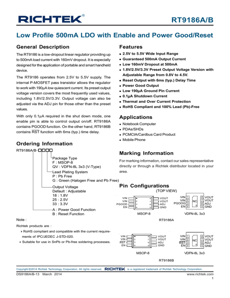
Ordering Information
RT9186A/B
Marking Information
Package Type
For marking information, contact our sales representative
F : MSOP-8
directly or through a Richtek distributor located in your
QV : VDFN-8L 3x3 (V-Type)
area.
Lead Plating System
P : Pb Free
G : Green (Halogen Free and Pb Free)
Output Voltage
Default : Adjustable
18 : 1.8V
25 : 2.5V
33 : 3.3V
A : Power Good Function
B : Reset Function
Pin Configurations
(TOP VIEW)
VIN
VIN
PGOOD
EN
8
2
7
3
6
4
5
VOUT
VOUT
ADJ
GND
VIN
VIN
PGOOG
EN
MSOP-8
Note :
1
2
3
4
NC
9
8
7
6
5
VOUT
VOUT
ADJ
GND
VDFN-8L 3x3
RT9186A
Richtek products are :
RoHS compliant and compatible with the current requirements of IPC/JEDEC J-STD-020.
Suitable for use in SnPb or Pb-free soldering processes.
VIN
VIN
RST
EN
8
2
7
3
6
4
5
VOUT
VOUT
ADJ
GND
MSOP-8
VIN
VIN
RST
EN
1
2
3
4
NC
9
8
7
6
5
VOUT
VOUT
ADJ
GND
VDFN-8L 3x3
RT9186B
Copyright © 2014 Richtek Technology Corporation. All rights reserved.
DS9186A/B-13 March 2014
is a registered trademark of Richtek Technology Corporation.
www.richtek.com
1
RT9186A/B
Function Pin Description
Pin Number
Pin Name
Pin Function
MSOP-8
VDFN-8L 3x3
1, 2
1, 2
3
3
3
3
4
4
EN
Enable Control Input (Active-High). There should be a pull low resistor
100k connected to GND when the control signal is floating.
5
5
GND
Ground.
6
6
ADJ
Output Voltage Setting. Connect to GND for Fixed output voltage
model.
7, 8
7, 8
VOUT
Output Voltage.
9
9
NC
No Internal Connection.
VIN
Power Input Voltage.
PGOOD
Power Good Indicator. (RT9186A).
(RT9186A)
Open-Drain Active-Low Reset Output. Connect a 100k to VOUT to
RST
obtain output voltage.
(RT9186B) In shutdown the RST output is low.
Typical Application Circuit
VIN
VIN
CIN
1µF
Enable
VOUT
RPGOOD/RST
100k
RT9186A/B
EN
PGOOD/RST
GND
VOUT
COUT
10µF
To C
ADJ
Figure 1. Fixed Voltage Regulator
VIN
Enable
VIN
CIN
1µF
VOUT
RT9186A/B
COUT
10µF
VOUT
RPGOOD/RST
100k
R1
PGOOD/RST
EN
GND
To C
ADJ
R2
VOUT
R1
0.8 (1
)
R2
Figure 2. Adjustable Voltage Regulator
Note1 : R2 should be less than 80k to ensure regulation.
μF is recommended for output stability.
Note2 : X5R or X7R input capacitor ≥ 1μ
Copyright © 2014 Richtek Technology Corporation. All rights reserved.
www.richtek.com
2
is a registered trademark of Richtek Technology Corporation.
DS9186A/B-13 March 2014
RT9186A/B
Function Block Diagram
VIN
Current Limit
Sensor
+
0.8V
Reference
Error
Amplifier
-
+
VOUT
Shutdown
Logic
EN
Thermal
Shutdown
ADJ
PGOOD
-
-
+
+
80%
Reference
100mV
Output Mode
Comparator
GND
-RT9186A-
VIN
Current Limit
Sensor
+
Error
Amplifier
0.8V
Reference
-
+
VOUT
Shutdown
Logic
EN
Thermal
Shutdown
ADJ
RST
-
-
+
Delay
Timer
+
80%
Reference
Output Mode
Comparator
100mV
GND
-RT9186B-
Copyright © 2014 Richtek Technology Corporation. All rights reserved.
DS9186A/B-13 March 2014
is a registered trademark of Richtek Technology Corporation.
www.richtek.com
3
RT9186A/B
Timing Diagram
VIN
80% of VOUT (Normal)
VOUT
PGOOD Function
(RT9186A)
Reset function
(RT9186B)
Delay Time (typ.) 6ms
Absolute Maximum Ratings
(Note 1)
Input Voltage ----------------------------------------------------------------------------------------------------------------- 7V
Storage Temperature Range --------------------------------------------------------------------------------------------Lead Temperature (Soldering, 10 sec.) -------------------------------------------------------------------------------Power Dissipation, PD @ TA = 25°C
MSOP-8 ---------------------------------------------------------------------------------------------------------------------VDFN-8L 3x3 ---------------------------------------------------------------------------------------------------------------Package Thermal Resistance (Note 2)
MSOP-8, θJA ----------------------------------------------------------------------------------------------------------------VDFN-8L 3x3, θJA ----------------------------------------------------------------------------------------------------------Junction Temperature -----------------------------------------------------------------------------------------------------ESD Susceptibility (Note 3)
HBM (Human Body Model) -----------------------------------------------------------------------------------------------
Recommended Operating Conditions
−65°C to 150°C
260°C
0.625W
0.952W
160°C/W
105°C/W
150°C
2kV
(Note 4)
Input Voltage ----------------------------------------------------------------------------------------------------------------- 2.5V to 5.5V
Junction Temperature Range --------------------------------------------------------------------------------------------- −40°C to 125°C
Ambient Temperature Range --------------------------------------------------------------------------------------------- −40°C to 85°C
Copyright © 2014 Richtek Technology Corporation. All rights reserved.
www.richtek.com
4
is a registered trademark of Richtek Technology Corporation.
DS9186A/B-13 March 2014
RT9186A/B
Electrical Characteristics
(VIN = VOUT(NOM) + 500mV or VIN = +2.5V (whichever is greater), TA = 25°C, unless otherwise specified)
Parameter
Symbol
Test Conditions
Min
Typ
Max
Unit
2.0
2.3
2.4
V
3
0
3
%
0.8
--
4.5
V
0.784
0.8
0.816
V
--
10
100
nA
General Specification
Input Under Voltage Lock-Out
VUVLO
Output Voltage Accuracy
(Preset Mode)
VOUT
Adjustable Output Voltage Range
VOUT_ADJ
ADJ Pin Voltage
VADJ
ADJ Input Bias Current
IADJ
VADJ = +0.8V
Short Circuit Current Limit
ILIM
VOUT = 0V
0.9
1.4
2.0
A
Quiescent Current (Note 5)
IQ
IOUT = 0mA
--
190
250
A
Dropout Voltage
VDROP
IOUT = 500mA
VOUT = 2.5V
--
200
330
VOUT = 3.3V
--
160
220
VLINE
VOUT + 0.1V VIN 5.5V
IOUT = 5mA
--
0.02
0.125
%/V
VLOAD
IOUT = 1mA to 500mA
--
21
40
mV
ISTBY
VIN = 5.5V
--
0.1
2
A
Logic-Low
VENL
VIN = 2.5V
--
--
0.7
Logic-High
VENH
VIN = 5.5V
1.6
--
--
IEN
VCE = 5.5V
--
20
100
nA
VOL
Reset Output Sinking 2mA
--
50
100
mV
Output High Leakage Current
VRST = 5V
--
--
100
nA
Threshold to Output Voltage
Rising edge, referred to VOUT
77
80
83
%
Rising edge of VOUT to VRST
0.7
6
8
ms
PGOOD Output Low Voltage
PGOOD Output sinking 2mA
--
50
100
mV
Output High Leakage Current
VPGOOD = 5V
--
--
100
nA
Threshold to Output Voltage
Rising edge, referred to VOUT
77
80
83
%
(Note 6)
Line Regulation
Load Regulation
(Note 7)
IOUT = 1mA to 500mA
mV
Chip Enable
Standby Current
EN Threshold
Voltage
EN Input Bias Current
V
Reset
Reset Output Low Voltage
Reset Delay Time
TDELAY
Power Good
Thermal Protection
Thermal Shutdown Temperature
TSD
--
160
--
C
Thermal Shutdown Hysteresis
TSD
--
30
--
C
Copyright © 2014 Richtek Technology Corporation. All rights reserved.
DS9186A/B-13 March 2014
is a registered trademark of Richtek Technology Corporation.
www.richtek.com
5
RT9186A/B
Note 1. Stresses beyond those listed “Absolute Maximum Ratings” may cause permanent damage to the device. These are
stress ratings only, and functional operation of the device at these or any other conditions beyond those indicated in
the operational sections of the specifications is not implied. Exposure to absolute maximum rating conditions may
affect device reliability.
Note 2. θJA is measured at TA = 25°C on a single-layer and four-layer test board of JEDEC 51. The measurement case position
of θJC is on the lead of the package.
Note 3. Devices are ESD sensitive. Handling precaution is highly recommended.
Note 4. The operating conditions beyond the recommended range is not guaranteed.
Note 5. Quiescent, or ground current, is the difference between input and output currents. It is defined by IQ = IIN - IOUT under
no load condition (IOUT = 0mA). The total current drawn from the supply is the sum of the load current plus the ground
pin current.
Note 6. The dropout voltage is defined as VIN -VOUT, which is measured when VOUT is VOUT(NORMAL) − 100mV.
Note 7. Regulation is measured at constant junction temperature by using a 20ms current pulse. Devices are tested for load
regulation in the load range from 1mA to 300mA and 500mA respectively.
Copyright © 2014 Richtek Technology Corporation. All rights reserved.
www.richtek.com
6
is a registered trademark of Richtek Technology Corporation.
DS9186A/B-13 March 2014
RT9186A/B
Typical Operating Characteristics
μF(X7R Ceramic), COUT = 10μ
μF(Y5V Ceramic), TA = 25°°C, unless otherwise specified.
CIN = 1μ
Input Voltage
Voltage
Output
Voltagevs.
vs.Output
Input Voltage
3.5
Output Voltage vs. Temperature
No Load
3.3
ILOAD = 500mA
2.5
2
1.5
1
0.5
0
2.7
3.4
4.1
4.8
VEN = VIN = 5V
RL =
2.9
2.7
VOUT = 2.5V
2.5
2.3
2.1
VOUT = 1.8V
1.9
VOUT = 3.3V
2
VOUT = 3.3V
3.1
Output Volatge (V)
Output Voltage (V)
3
1.7
5.5
-50
-25
0
Input Voltage (V)
Quiescent Current vs. Temperature
VEN = VIN = 3.3V
VOUT = 1.8V
RL =
210
190
170
150
75
100
125
VOUT = 2.5V
TJ = 125°C
200
150
TJ = 25°C
100
TJ = −40°C
50
0
130
-50
-25
0
25
50
75
100
0
125
100
200
Temperature (°C)
2
1.5
1
0.5
0
Time (1ms/Div)
400
500
Short Circuit Current Limit vs. Temperature
1.60
Short Circuit Current Limit (A)1
VEN = VIN = 3.3V
VOUT = 1.8V
RL = 0 Ω
300
Load Current (mA)
Short Circuit Current Limit
Short Circuit Current Limit (A)
50
Dropout Voltage vs. Load Current
250
Dropout Voltage (mV)
Quiescent Current (µA) 1
230
25
Temperature (°C)
VEN = VIN = 3.3V
VOUT = 1.8V
RL = 0 Ω
1.55
1.50
1.45
1.40
-50
-25
0
25
50
75
100
125
Temperature (°C)
Copyright © 2014 Richtek Technology Corporation. All rights reserved.
DS9186A/B-13 March 2014
is a registered trademark of Richtek Technology Corporation.
www.richtek.com
7
RT9186A/B
Output Voltage
Deviation(mV)
20
0
-20
4
3
Load Transient Response
Load
Current (A)
Input
Voltage(V)
Output Voltage
Deviation(mV)
Line Transient Response
ILOAD = 100mA
VOUT = 1.8V
Without CIN
20
0
-20
0.4
0.2
0
VOUT = 1.8V
VIN = 3.3V
ILOAD = 1 to 250mA
Time (50μs/Div)
Time (50μs/Div)
Reset Response
Reset Response
VEN (2V/Div)
ILOAD = 50mA
VOUT = 3.3V
VIN = 3.8V
VIN = VEN (2V/Div)
VOUT (2V/Div)
VOUT (2V/Div)
VRST (2V/Div)
ILOAD = 50mA
VOUT = 3.3V
Without CIN
VRST (2V/Div)
Time (10ms/Div)
Time (1ms/Div)
PGOOD Response
Shutdown Response
ILOAD = 50mA
VOUT = 3.3V
VIN = 3.8V
VOUT (2V/Div)
ILOAD = 500mA, VOUT = 3.3V, VIN = 5V
EN Voltage
(V)
VEN (2V/Div)
4
2
0
Output
Voltage (V)
3
VPGOOD (2V/Div)
2
1
0
Time (1ms/Div)
Copyright © 2014 Richtek Technology Corporation. All rights reserved.
www.richtek.com
8
Time (100μs/Div)
is a registered trademark of Richtek Technology Corporation.
DS9186A/B-13 March 2014
RT9186A/B
Application Information
Capacitor Selection and Regulator Stability
Input-Output (Dropout) Voltage
Careful selection of the external capacitors for RT9186 is
highly recommended in order to remain high stability and
performance.
A regulator's minimum input-to-output voltage differential
Regarding the Input capacitor, connecting an X7R or X5R
ceramic capacitor which is ≥ 1μF between input and ground
is a must. Distance less than 1 cm between input pin and
ground of RT9186 is recommended to avoid any unstability.
With larger value of capacitor adding on lower ESR could
result in better performance for both PSRR and line
transient response.
Regarding the output capacitor, connecting a10μF
capacitor between output and ground is a must. Any
capacitor is acceptable only with a highlight of relation
between ESR region and Load current, shown in below.
Output capacitor with larger capacitance can reduce noise
and improve load transient response, stability, and PSRR.
The same as Input capacitor, distance less than 1 cm
between output pin and ground of RT9186 is recommended
to avoid any unstability.
Region of Stable COUT ESR vs. Load Current
100.00
100
VIN = 3V
COUT ESR (Ω)
10.00
10
Instable
(dropout voltage) determines the lowest usable supply
voltage. In battery-powered systems, this determines the
useful end-of-life battery voltage. Because the device uses
a P-MOSFET, its dropout voltage is a function of drain-tosource on-resistance, RDS(ON), multiplied by the load
current :
VDROPOUT = VIN − VOUT = RDS(ON) IOUT
Over-Current and Short-Circuit Protection
The RT9186 continuously monitors output current to
provide maximum safety. In the event of output over current
or short-circuit, over-current protection function will activate
and override the voltage regulation function to limit output
current at 1.4A typically. Large power dissipation at this
condition may cause chip temperature to raise and trigger
the over temperature protection if over-current or shortcircuit is not removed in a short time
Power Good and Reset
The power good and the reset output is an open-drain
output. Connect an 100kΩ pull up resistor to VOUT to obtain
an output voltage. The power good will output high
immediately after the output voltage arrives 80% of normal
output voltage. In the same situation, the reset will output
high with 6ms delay time. See Timing Diagram and Typical
Operating Characteristics.
1.001
Adjustable Operation
Stable
The output voltage of RT9186 is adjustable from 0.8V to
4.5V by an external voltage divider as shown in Typical
Application Circuit Figure 2. The value of R2 should be
less than 80kΩ to ensure regulation.
0.10
0.10
Instable
0.01
0.01
0
100
200
300
400
Load Current (mA)
500
Chip Enable Operation
Pull the EN pin low to drive the device into shutdown mode.
At the same time, pin 3 (PGOOD/RST) is pulled low. During
shutdown mode, the standby current drops to 0.1μA (typ).
The output voltage decay rate is determined by the external
capacitor and load current. Drive the EN pin high to turn
on the device again.
Copyright © 2014 Richtek Technology Corporation. All rights reserved.
DS9186A/B-13 March 2014
is a registered trademark of Richtek Technology Corporation.
www.richtek.com
9
RT9186A/B
Reverse Current Path
The P-MOSFET pass element of RT9186 has an
inherendiode connected between the regulator input and
output as shown in Figure 3. The inherent diode will be
forward biased and conduct an unlimited current if VOUT is
sufficiently higher than V IN . a Schottky diode is
recommended connecting parallel with the inherent diode
in the application where output voltage may be higher than
input voltage as shown in Figure 4. This Schottkly will
clamp the forward bias voltage to 0.3V and conduct the
possible current to protect the RT9186 from damage by
unlimited current.
VIN
VOUT
Figure 3. Inherent Diode of P-MOSFET Pass Transistor
The maximum power dissipation depends on the thermal
resistance of IC package, PCB layout, the rate of
surroundings airflow and temperature difference between
junction to ambient. The maximum power dissipation can
be calculated by following formula :
PD(MAX) = (TJ(MAX) − TA) / θJA
Where T J(MAX) is the maximum operation junction
temperature 125°C, TA is the ambient temperature and the
θJA is the junction to ambient thermal resistance.
For recommended operating conditions specification of
RT9186A/B, where TJ(MAX) is the maximum junction
temperature of the die (125°C) and TA is the maximum
ambient temperature. The junction to ambient thermal
resistance θJA is layout dependent. For VDFN-8L 3x3
package, the thermal resistance θJA is 105°C/W on the
standard JEDEC 51-3 single-layer 1S thermal test board
and 70°C/W on the standard JEDEC 51-7 4-layers 2S2P
thermal test board. The maximum power dissipation at
TA = 25°C can be calculated by following formula :
PD(MAX) = (125°C − 25°C) / 105 = 0.952W for single-layer
1S board
VOUT
Figure 4. Schottkly Diode Parallel with The Ingerent Diode
Thermal Considerations
Thermal protection limits power dissipation in
RT9186A/B. When the operation junction temperature
exceeds 160°C, the OTP circuit starts the thermal
shutdown function and turns the pass element off. The
pass element turn on again after the junction temperature
cools by 30°C.
For continuous operation, do not exceed absolute
maximum operation junction temperature 125°C. The
power dissipation definition in device is :
PD = (VIN − VOUT) x IOUT + VIN x IQ
The maximum power dissipation depends on operating
ambient temperature for fixed T J(MAX) and thermal
resistance θJA. The Figure 5 of derating curves allows the
designer to see the effect of rising ambient temperature
on the maximum power allowed.
Maximum Power Dissipation (mW)
VIN
PD(MAX) = (125°C − 25°C) / 70 = 1.428W for 4-layers
2S2P board
1500
DFN-8L at 4-Layers PCB
1250
DFN-8L at 1-Layers PCB
1000
750
500
MSOP-8 at 1-Layers PCB
250
0
0
25
50
75
100
125
Ambient Temperature (°C)
Figure 5
Copyright © 2014 Richtek Technology Corporation. All rights reserved.
www.richtek.com
10
is a registered trademark of Richtek Technology Corporation.
DS9186A/B-13 March 2014
RT9186A/B
Layout Consideration
Good board layout practices must be used or instability
can be induced because of ground loops and voltage drops.
The input and output capacitors MUST be directly
connected to the input, output, and ground pins of the
device using traces which have no other currents flowing
through them.
The best way to do this is to layout CIN and COUT near the
device with short traces to the VIN, VOUT, and ground pins.
The regulator ground pin should be connected to the
external circuit ground so that the regulator and its
capacitors have a “single point ground”.
It should be noted that stability problems have been seen
in applications where “vias” to an internal ground plane
were used at the ground points of the device and the input
and output capacitors. This was caused by varying ground
potentials at these nodes resulting from current flowing
through the ground plane. Using a single point ground
technique for the regulator and it’ s capacitors fixed the
problem. Since high current flows through the traces going
into VIN and coming from VOUT, Kelvin connect the capacitor
leads to these pins so there is no voltage drop in series
with the input and output capacitors.
Optimum performance can only be achieved when the
device is mounted on a PC board according to the
MSOP-8 Board Layout diagram.
GND
+
SET
VOUT
PGOOD
/ RST
EN
VIN
+
GND
MSOP-8 Board Layout
Copyright © 2014 Richtek Technology Corporation. All rights reserved.
DS9186A/B-13 March 2014
is a registered trademark of Richtek Technology Corporation.
www.richtek.com
11
RT9186A/B
Outline Dimension
D
L
E1
E
e
A2
A
A1
b
Dimensions In Millimeters
Dimensions In Inches
Symbol
Min
Max
Min
Max
A
0.810
1.100
0.032
0.043
A1
0.000
0.150
0.000
0.006
A2
0.750
0.950
0.030
0.037
b
0.220
0.380
0.009
0.015
D
2.900
3.100
0.114
0.122
e
0.650
0.026
E
4.800
5.000
0.189
0.197
E1
2.900
3.100
0.114
0.122
L
0.400
0.800
0.016
0.031
8-Lead MSOP Plastic Package
Copyright © 2014 Richtek Technology Corporation. All rights reserved.
www.richtek.com
12
is a registered trademark of Richtek Technology Corporation.
DS9186A/B-13 March 2014
RT9186A/B
D2
D
L
E
E2
1
e
SEE DETAIL A
b
2
1
2
1
A
A1
A3
DETAIL A
Pin #1 ID and Tie Bar Mark Options
Note : The configuration of the Pin #1 identifier is optional,
but must be located within the zone indicated.
Symbol
Dimensions In Millimeters
Dimensions In Inches
Min
Max
Min
Max
A
0.800
1.000
0.031
0.039
A1
0.000
0.050
0.000
0.002
A3
0.175
0.250
0.007
0.010
b
0.200
0.300
0.008
0.012
D
2.950
3.050
0.116
0.120
D2
2.100
2.350
0.083
0.093
E
2.950
3.050
0.116
0.120
E2
1.350
1.600
0.053
0.063
e
L
0.650
0.425
0.026
0.525
0.017
0.021
V-Type 8L DFN 3x3 Package
Richtek Technology Corporation
14F, No. 8, Tai Yuen 1st Street, Chupei City
Hsinchu, Taiwan, R.O.C.
Tel: (8863)5526789
Richtek products are sold by description only. Richtek reserves the right to change the circuitry and/or specifications without notice at any time. Customers should
obtain the latest relevant information and data sheets before placing orders and should verify that such information is current and complete. Richtek cannot
assume responsibility for use of any circuitry other than circuitry entirely embodied in a Richtek product. Information furnished by Richtek is believed to be
accurate and reliable. However, no responsibility is assumed by Richtek or its subsidiaries for its use; nor for any infringements of patents or other rights of third
parties which may result from its use. No license is granted by implication or otherwise under any patent or patent rights of Richtek or its subsidiaries.
DS9186A/B-13 March 2014
www.richtek.com
13


