DC1354A - Linear Technology
advertisement

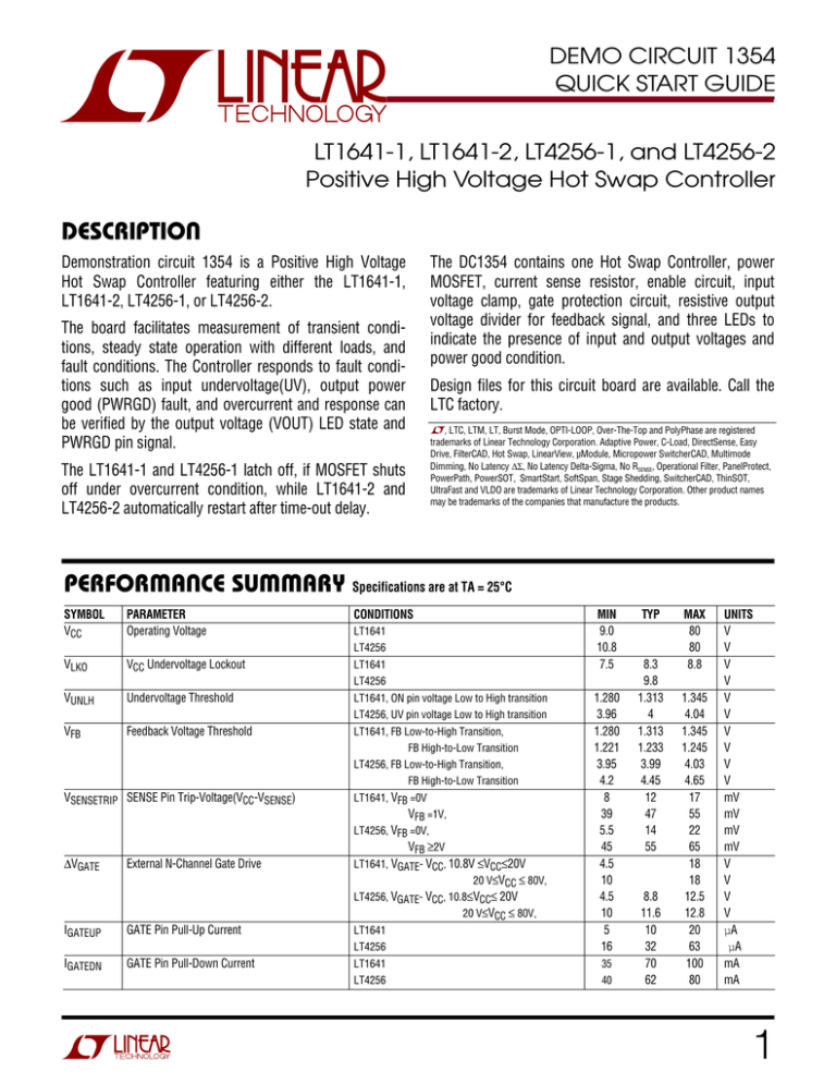
DEMO CIRCUIT 1 3 5 4 LT1641-1, LT1641-2, LT4256-1, AND LT4256-2 Q UICK S TA RT G UIDE L T1 6 4 1 -1 , L T1 6 4 1 -2, L T4 25 6 -1 , a n d L T4 25 6 -2 P o s itiv e H ig h V o lta g e H o t S w a p Co n tro lle r DESCRIPTION The DC1354 contains one Hot Sw ap Controller, pow er M OSFET, current sense resistor, enable circuit, input voltage clamp, gate protection circuit, resistive output voltage divider for feedback signal, and three LEDs to indicate the presence of input and output voltages and pow er good condition. Demonstration circuit 1354 is a Positive High Voltage Hot Sw ap Controller featuring either the LT1641-1, LT1641-2, LT4256-1, or LT4256-2. The board facilitates measurement of transient conditions, steady state operation w ith different loads, and fault conditions. The Controller responds to fault conditions such as input undervoltage(UV), output pow er good (PW RGD) fault, and overcurrent and response can be verified by the output voltage (VOUT) LED state and PW RGD pin signal. Design files for this circuit board are available. Call the LTC factory. L, LTC, LTM , LT, Burst M ode, OPTI-LOOP, Over-The-Top and PolyPhase are registered trademarks ofLinear Technology Corporation. Adaptive Pow er, C-Load, DirectSense, Easy Drive, FilterCAD, Hot Sw ap, LinearView , µM odule, M icropow er Sw itcherCAD, M ultimode Dimming, No Latency , No Latency Delta-Sigma, No R SENSE, Operational Filter, PanelProtect, Pow erPath, Pow erSOT, SmartStart, SoftSpan, Stage Shedding, Sw itcherCAD, ThinSOT, UltraFast and VLDO are trademarks ofLinear Technology Corporation. Other product names may be trademarks ofthe companies that manufacture the products. The LT1641-1 and LT4256-1 latch off, if M OSFET shuts off under overcurrent condition, w hile LT1641-2 and LT4256-2 automatically restart after time-out delay. PERF ORM A NCE SU M M A RY Specifications are atTA = 25°C SYM BOL VCC PAR AM ETER Operating Voltage LT1641 VLKO VCC Undervoltage Lockout CON DITION S M IN 9.0 10.8 7.5 LT4256 LT1641 LT4256 VUNLH Undervoltage Threshold LT4256 1.280 3.96 1.280 1.221 3.95 4.2 8 39 5.5 45 4.5 10 4.5 10 5 16 LT1641 35 LT4256 40 LT1641, O N pin voltage Low to High transition LT4256, U V pin voltage Low to High transition VFB Feedback Voltage Threshold LT1641, FB Low -to-High Transition, FB High-to-Low Transition LT4256, FB Low -to-High Transition, FB High-to-Low Transition VSENSETRIP SENSE Pin Trip-Voltage(VCC-VSENSE) LT1641, VFB =0V VFB =1V, LT4256, VFB =0V, ∆VGATE External N-Channel Gate Drive VFB ≥2V LT1641, VGATE- VCC, 10.8V ≤VCC≤20V 20 V≤VCC ≤ 80V, LT4256, VGATE- VCC, 10.8≤VCC≤ 20V 20 V≤VCC ≤ 80V, IGATEUP IGATEDN GATE Pin Pull-Up Current GATE Pin Pull-Dow n Current LT1641 TYP 8.3 9.8 1.313 4 1.313 1.233 3.99 4.45 12 47 14 55 8.8 11.6 10 32 70 62 M AX 80 80 8.8 1.345 4.04 1.345 1.245 4.03 4.65 17 55 22 65 18 18 12.5 12.8 20 63 100 80 UNITS V V V V V V V V V V mV mV mV mV V V V V µA µA mA mA 1 LT1641-1, LT1641-2, LT4256-1, AND LT4256-2 OPERA TING PRINCIPL ES The LT1641-1, LT1641-2, LT4256-1, and LT4256-2 are Positive High Voltage Hot Sw ap Controllers that have absolute maximum supply voltage (VCC) 100V and operating range (9-80) V for LT1641 and (10.8-80) V for LT4256. In the DC1354A any controller operates on the +48V rail. Each board can easily be readjusted for any rated voltage by replacing the enable circuit (R5, R11), input voltage clamp (D1), gate protection circuit (R8, R14, D3, D6), and resistive output voltage divider (R10, R12). The DC1354A as supplied by the factory is assembled w ith the SUM 90N10-8m2p M OSFET in a D2PAK package and 7mΩ current sense resistor (R1). Q U ICK STA RT PROCEDU RE Demonstration circuit DC1354 is easy to set up to evaluate the performance of the LT1641-1, LT1641-2, LT4256-1, and LT4256-2. Refer Figure 1 for proper measurement equipment setup and follow the procedure below . The board test is performed in several steps by measuring some transient parameters and verifying successful or failed pow er up actions under defined conditions. In all test steps turn on sw itch SW _PS to connect demo board to the +48V pow er supply, turn on sw itch SW _PS to activate controller (connecting the ENABLE pin to the VIN +48V) and turn +48V off for resetting controller after fault. 1. It should be noted that loading parameters such as Low Capacitive Load, H igh Capacitive Load, Low R esistive Load, and H igh R esistive are different for LT4256 and for LT1641. These parameters are show n below separately for each controller: LTC1641 ● Low Capacitive load 1000uF, ● High Capacitive load 8700uF, ● Low Resistive load 10 Ω, 50W , ● High Resistive load 5.5 Ω . LTC4256 ● Low Capacitive load 250uF, ● High Capacitive load 3500uF, ● Low Resistive load 11 Ω, 50W , 2 ● High Resistive load 5.0 Ω . 2. Place a scope probe to the VO U T turret, turn on controller, and measure a pow er-up time w ith no load. For LT4256 this time must be in the range (13.7 - 54) ms, and for LT1641- (43 - 173) ms. 3. Connect Low Capacitive Load to the output of hot sw ap circuitry (VO U T +48V turret). Turn on controller. This pow er up should be successful and tw o LEDs (VO U T – green - and PW R GD - orange) must light. NOTE. The follow ing tests verify loaded Controller performance. The transients w ith Low Load should be successfully completed, w hile transients w ith High Load should fail. The LT1641-1 and LT4256-1 in the overcurrent fault condition are latched off, w hile the LT1641-2 and LT4256-2 provide retry. To avoid pow er M OSFET damage in the LT16412 and LT4256-2 High Load tests keep sw itch SW _ON in the on position very short time. 4. Connect H igh Capacitive Load to the output of hot sw ap circuitry (VO U T +48V turret). Turn on controller. This pow er up should be unsuccessful, and tw o LEDs remaining offw ill confirm this. For LT4256-1 and LT1641-1 the failed pow er-up is indicated by the VOUT (green) and PW RGD (orange) LED lights remaining off. Disconnect the ENABLE turret from the VIN +48V turret for short time and connect them again. The controller should be latched off in the shut offmode, For LT4256-2 and LT1641-2 make short time connection of the ENABLE turret and VIN +48V. The VOUT (green) and PW RGD (orange) LED w ill blink indicating an autoretry in the failed pow er up. LT1641-1, LT1641-2, LT4256-1, AND LT4256-2 5. Load output w ith Low R esistive Load. Controller should successfully keep this load. 6. Turn controller on. Load output w ith H igh R esistive Load. Controller should fail to keep this load. NOTE. In the designing ofthe pow er-up transient w ith mentioned Controllers special attention should be paid to correspondence betw een pow er M OSFET safe operating area and transient parameters (current limit level, duration ofthe transient, relationship betw een capacitive load and resistive load and timer period). 7. Verify that controller alive after overload test. Figure 1. Proper M easurem entEquipm entSetup 3 LT1641-1, LT1641-2, LT4256-1, AND LT4256-2 4


