Tayloe Mixer
advertisement

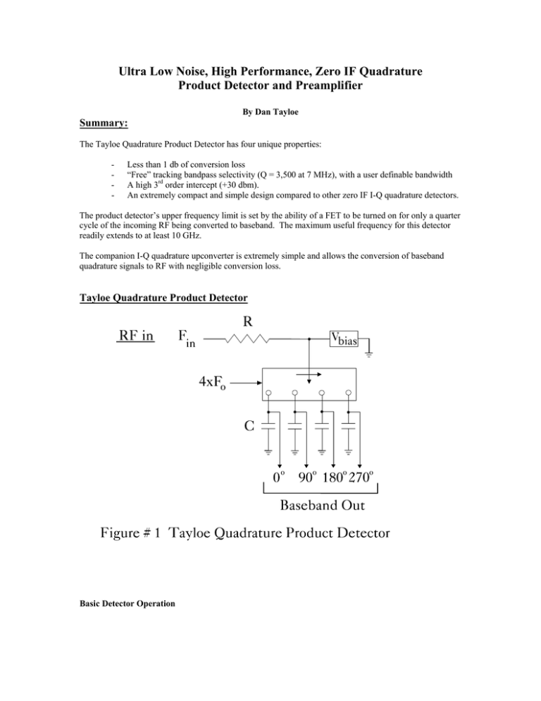
Ultra Low Noise, High Performance, Zero IF Quadrature Product Detector and Preamplifier By Dan Tayloe Summary: The Tayloe Quadrature Product Detector has four unique properties: - Less than 1 db of conversion loss “Free” tracking bandpass selectivity (Q = 3,500 at 7 MHz), with a user definable bandwidth A high 3rd order intercept (+30 dbm). An extremely compact and simple design compared to other zero IF I-Q quadrature detectors. The product detector’s upper frequency limit is set by the ability of a FET to be turned on for only a quarter cycle of the incoming RF being converted to baseband. The maximum useful frequency for this detector readily extends to at least 10 GHz. The companion I-Q quadrature upconverter is extremely simple and allows the conversion of baseband quadrature signals to RF with negligible conversion loss. Tayloe Quadrature Product Detector Basic Detector Operation The basic product detector is shown in figure # 1. Note that the detector is extremely simple in design. The incoming RF signal is routed via a common resistor, R and a commutating RF multiplexer, to one of four detection capacitors, C. This 1-of-four multiplexer is commutated at a rate of four times the desired detection frequency. The 4x commutating frequency causes each capacitor to see a quarter cycle of the input RF at the desired detection frequency. Mixers generally produce sum and difference outputs. In zero IF applications, the difference frequency is used, while the sum is thrown away. Therefore, the conversion loss using an ideal mixer is at least 3 db, with a typical conversion loss of 4-6 db in practice. Conversely, this design is not a mixer, but rather can best be described as a “switching integrator”, producing only a difference frequency. The input R and a particular detection C act together as an integrator, averaging the signal over the quarter cycle sample to the detection capacitor. Figure # 2 shows a sine wave that happens to be the same frequency as the detector is tuned to, and with the phasing alignment that will produce a maximum positive voltage on the first capacitor, zero volts on the second and fourth capacitor, and a maximum negative voltage on the third capacitor. Performing an integration over the peak quarter cycle of this sine wave shows that the maximum detected voltage will be approximately 0.9002 times the peak voltage of the sine wave. Hence, the detection loss is about 0.9 db. If the frequency of the incoming signal is shifted slightly from being exactly the detection frequency, the resulting voltages on the detection capacitors will no longer be stationary, but will drift with time, following the difference frequency between the incoming signal and the detection frequency. In short, the first capacitor becomes a baseband product detector sampling at 0 degrees, with the other detection capacitors detecting at 90, 180, and 270 degrees respectively. 2 The 180 and 270 degree outputs carry information that is redundant with the 0 and 90 degree outputs. Therefore the 0 and 180 degree outputs can be summed differentially to produce a single composite Inphase (“I”) signal and 90 and 270 can be likewise combined to form a Quadrature (“Q”) signal. See figure # 3. This differential summing can be performed using low noise op-amps or instrumentation amps. Detection Bandwidth The detector has a frequency roll off that can be set by properly selecting R and C. Together R and C act like a lowpass filter at baseband. However, all components of the series resistance must be taken into consideration when computing the frequency roll off. See figure # 4. Notice that the equivalent series resistance is not just the filter input R, but also includes the system input impedance, Rsys, and the switch resistance Rswitch. Since each detector capacitor sees the input for only a quarter of the time, the effective resistance used in the low pass filter calculation is: 4 times (Rsys + R + Rswitch). 3 Suppose a 1 KHz detection bandwidth is desired for a 7 MHz receiver. If Rsys is 50 ohms, and both R and Rswitch are assumed to be zero, a detection C of 1.33 uf yields a 3 db lowpass filter bandwidth of 1 KHz. Notice that the actual detection bandwidth will be 2 KHz since the lowpass roll off will extend to both sides of the center detection frequency. However, a selection of 01.33 uf will cause the edges to be 3 db down, so the actual selection of C will depend upon a potential trade off in the wide band adjacent channel rejection and the roll off of the actual signal at the detection edge. Note that the detection bandwidth tracks with the frequency the detector is set to. Even though the roll off represents only a single R/C pole at base band, a 2 KHz tracking bandwidth at 7 MHz is equivalent to a single pole tuned circuit Q of 3500. At 28 MHz, the same 2 KHz tracking bandwidth yields a Q of 14,000. It is typical that a receiver is designed to select one signal out of a number of signals spread out over a desired frequency spectrum. In order for the detector and subsequent stages to guard against undesired out of band signals, bandpass filtering is often used as the first stage in a receiver’s front end. This bandpass filtering is normally fixed tuned and as such provides no in band protection from other signals within the desired frequency band. In contrast, the selectivity provided by this detector is centered about the detection frequency. As such the selectivity it provides is superior to that provided by band wide bandpass filtering, providing some margin of “free” selectivity against both adjacent channel and out of band signals. In some cases, this built in selectivity may significantly reduce or even negate the need for any receiver front end bandpass filtering and it associated additional insertion loss. However, at a minimum, lowpass filtering is required to protect the mixer from detecting harmonics of the desired frequency, particularly the second (-40 db down) and odd order harmonics. This lowpass filter is usually required to eliminate harmonics from the associated transmitter and normally has minimal insertion loss at the transmit frequency. By having the transmitter and receiver share the same low pass filter, both total system cost and receiver front end insertion loss can be minimized. Detection Noise – A Design Evolution The above diagram represents the first evolution of the Tayloe detector connected to a post detector preamplifier operational amplifier. Note that the preamplifier is AC coupled to the detector. Taking the fact that resistors generate unwanted noise, degrading the ultimate receiver sensitivity, the design has gone through several evolutionary steps to reduce dependency upon resistors in the critical path from the antenna to the preamplifier differential inputs. 4 In this step, the input 50 ohm resistor has been eliminated. Thus the detection bandwidth is now primarily a function of the input system resistance, assumed here as 50 ohms. The elimination of this resistance has both reduced loss and decreased the input noise level. This version has gone one step further and eliminated the input resistors into the preamplifier operational amplifiers. The input resistors are replaced by the system resistance as seen on the detector capacitor side of the detector. For a 50 ohm system, this is nominally 200 ohms. One result of eliminating the input resistors is that the gain of the preamplifiers has doubled, so the feedback resistors have been reduced to compensate. This configuration is close to ideal, but the resistors used to bias the non-inverting inputs will appear in parallel with the 200 ohms of detector capacitor side effective system resistance as a 200 ohms noise source. The noise from even 200 ohms of resistance is significant for very low noise cases. 5 This is the final version of the detector/preamplifier combination. Notice that preamplifier draws its bias from a direct connection to the detector. Note that the detector bias on the input side of the detector appears at each of the four detector capacitor outputs. A double balanced version of the detector is possible as well, as shown in the following figure Two separate detectors are driven with the inputs 180 degrees apart using an input transformer. The two detectors use a common set of four detector caps. Since the outputs of the two detectors are 180 degrees out of phase, the detector capacitors are now driven two at a time. 6 Noise Analysis of the Optimum Detector/Preamplifier Configuration In the optimum configuration, there are no resistors on the path from the antenna all the way to the input side of the preamplifier operational amplifier. The noise contribution of the feedback resistor is normally swamped by the output noise of the preamplifier as long as it has sufficient gain. The system noise at the RF input is expressed as: –174 + 10log(Bw) dbm or 0.45 nV/Sqrt(Bw) where Bw is the receiver bandwidth in Hz. At each of the four inputs to the preamplifiers, the noise seen as the system noise is reduced by the 0.9x (also 0.9 db) loss of the detector. Now assume that both pre-amplifiers each have the same gain, G, and a built in noise, Np. At the output of each of the preamplifiers, there will be one noise term for the preamplifier, and two for the system noise as seen by each of the two inputs. For a single preamplifier output, this noise will be: Sqrt( (2*0.9*0.45)**2 + (Np)**2)*G*Sqrt(Bw) If the outputs of both preamplifiers are used to produce a single composite signal, the composite noise term will be: Sqrt( (4*0.9*0.45)**2 + 2*(Np)**2)*G*Sqrt(Bw) On the other hand, the signal output for a signal input S will be: 0.9*S*4*G Both the signal and noise equations include the 0.9 db loss of the detector. Using the equations above, actual practice shows the sensitivity to be limited by the 0.9 db loss of the detection process and the noise of the first baseband preamplifier. Sample Noise Calculations Between the noise equation, and the signal equation, the input signal level necessary to produce an output signal equal to the output noise can be found: 0.9*S*4*G = G*Sqrt((4*0.9*0.45)**2 + 2*(Np)**2)*Sqrt(Bw) Or S = Sqrt((4*0.9*0.45)**2 + 2*(Np)**2)*Sqrt(Bw) / (0.9*4) It is instructive to compare the system input noise to the signal level required to reach a 3 db S+N/N ratio. Such a table is shown below for a receiver with a 1000 Hz bandwidth. System Noise @ Bw=1000Hz 14.2 nV / -143.8 dbm 14.2 nV / -143.8 dbm 14.2 nV / -143.8 dbm 14.2 nV / -143.8 dbm 14.2 nV / -143.8 dbm Preamplifier Noise (nV/SqrtHz) 9 4 2 1 0.8 Signal level for 3 db S+N/N 113 nV / -125.8 dbm 55.3 nV / -132.0 dbm 34.8 nV / -136.0 dbm 27.3 nV / -138.1 dbm 17.3 nV / -142.1 dbm The last entry demonstrates the importance of a very low noise baseband preamplifier on the overall sensitivity of the receiver. The sensitivity of the receiver is now a function of the noise of the preamplifier operational amplifier. The current state of the art in ultra low noise operational amplifiers has noise levels in the 0.8 nV/SqrtHz range. This is represented by such devices as the Linear Technology LT1115. Notice that when the detector is couple with an ultra low noise device such as this, it is practical to produce a receiving system that can receive a signal with a 3 db S+N/N that is only 1.7 db above the system noise without the use of an RF preamp. Furthermore, the fact that this baseband preamplifier is setting behind the bandpass characteristics of the detector makes it significantly less susceptible to other large in band signals than the typical receiver design which uses an unprotected RF amplifier in front of a broadband detector. Selective Single Image Reception If base band phasing is applied to the detected signals so as to provide for single sided reception, such as Single Sideband, the detector can be made to reverse the detection side (Upper Sideband vs. Lower Sideband) by reversing the direction of the rotation of the analog switch. 0 degrees becomes 270 degrees, 90 becomes 180, 180 becomes 90, and 270 becomes 0 degrees. Practically speaking, if a two-bit counter is used to select the switch outputs, inverting these bits will reverse the switching order, and thus the detected sideband. Comments This detector was built and tested. A dual band 7 and 3.5 MHz 5w prototype transceiver was constructed for personal amateur radio hobby use. The concept worked well. Using a TI 74CBT3253 (a dual 4:1 multiplexing memory bus switch device) as the detector’s 1-of-4 analog mux, a third order intercept of +30 dbm was obtained. Even though the prototype receiver had 115 db of gain at baseband, no problems with feedback were experienced. This is due primarily to the fact that the detector output is a rather large C to ground. This causes this most feedback sensitive point in the circuit to have a relatively low impedance, decreasing the likelihood of undesired feedback. With the free bandpass tracking selectivity (Q=3500+), 0.9 db RF to baseband conversion loss, and a high dynamic range of the detector (+30 dbm third order intercept), it may be possible to construct a very high performance, very low noise receiver without the use of a low noise RF preamp or a bandpass filter, all while using fewer parts and lowering cost. Quadrature Upconverter Basic Operation The quadrature upconverter is essentially the Tayloe quadrature product detector run backwards. See figure # 5. In it simplest form, neither the detector capacitors nor the resistor are required. Quadrature baseband inputs (0, 90, 180, and 270 degrees) are switched on for a quarter cycle each in sequence at the desired RF frequency, just like the detector. The resulting RF signal needs only some filtering (lowpass or bandpass) to fuse the quadrature pieces back together at the new frequency. 10 Except for the switch and the filter losses, the upconversion process itself is essentially lossless. The losses in the switch and the filter can be minimized. The quadrature upconverter requires as an input all four baseband phases. However, high speed inverting op-amps or simple differential drivers make it easy to create a 180 and 270 degree signals from the normal 0 degree “I” and 90 degree “Q” signals, as show above in figure # 5. I have since discovered that this upconverter is not new, and has been used with other four phase 90 degree networks to produce SSB signals. Devices such as the 74CBT3253 should allow up to 100 mw of SSB RF energy to be generated directly from phase shifted audio outputs, using no RF amplification. Comments The quadrature upconverter was also built and tested. A “sort of superhet” was built to test this idea. A Tayloe product detector was used to convert a RF signal to a four phase quadrature baseband signal in order to provide a signal source for the quadrature upconverter. These baseband signals were run through the quadrature upconverter to an IF frequency where the up converted signal was filtered, amplified, brought back to audio, and amplified to speaker level. Again, the concept was proven out. The low 1 db loss of the Tayloe quadrature product detector, combined with the almost lossless up conversion process of the quadrature upconverter, allowed the construction of an ultra low noise, superhet like receiver, with none of the usual IF images or mixer spurs. Despite testing the quadrature upconverter in a receiver setting, the upconverter is ideal as a transmitter companion to the receiver quadrature product detector. It may be desirable to keep the capacitors on the quadrature upconverter inputs for higher power transmitter upconversion purposes. The switching demands will extract extremely short duration, RF quarter cycle “bursts” of signal to be transferred from baseband to the RF side of the switch. A capacitor will help to store energy for these bursts, allowing the baseband drivers to provide a more averaged high level signal output power. Just like the product detector, if the up converter inputs are run backwards, the frequency sense of the outputs will be reversed. This could be used to selectively generate either Upper Sideband or Lower Sideband signals from one baseband quadrature signal. Likewise, in receiver applications as outlined 11 above, the IF filter can be switched from detecting Upper Sideband to Lower Sideband by simply reversing the direction of rotation in either the quadrature upconverter or in the quadrature product detector. If anyone has any further questions, I can be reached via email at Dan_Tayloe-P26412@email.mot.com. 12


