High-Speed Mechanically Flexible Single-Crystal Silicon Thin
advertisement

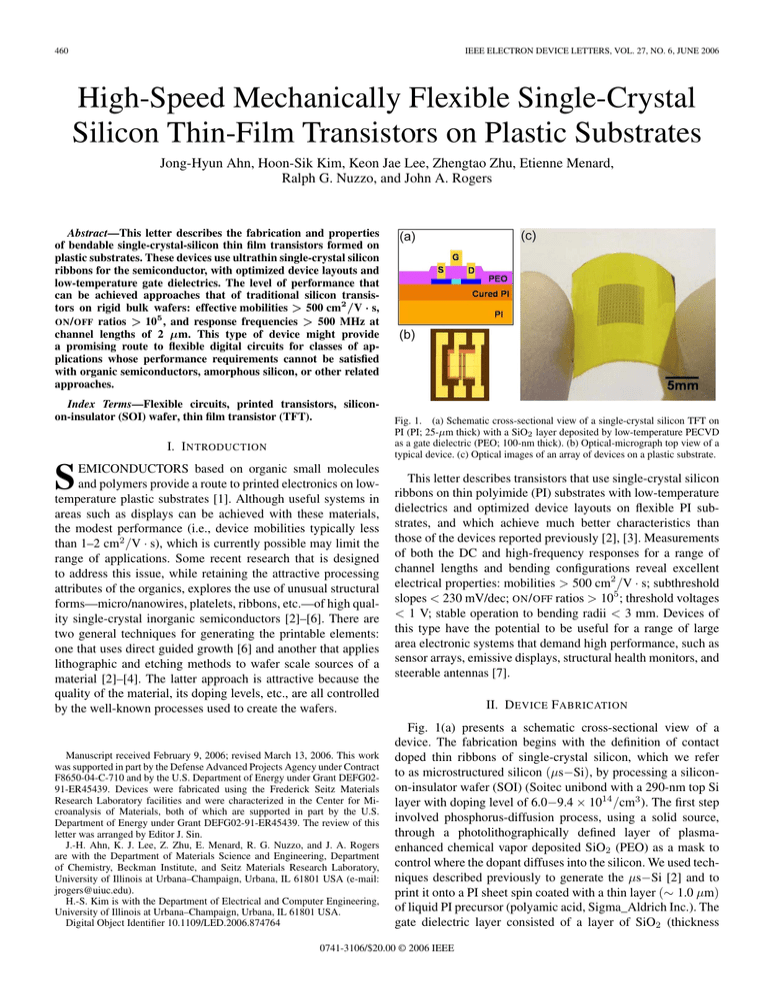
460 IEEE ELECTRON DEVICE LETTERS, VOL. 27, NO. 6, JUNE 2006 High-Speed Mechanically Flexible Single-Crystal Silicon Thin-Film Transistors on Plastic Substrates Jong-Hyun Ahn, Hoon-Sik Kim, Keon Jae Lee, Zhengtao Zhu, Etienne Menard, Ralph G. Nuzzo, and John A. Rogers Abstract—This letter describes the fabrication and properties of bendable single-crystal-silicon thin film transistors formed on plastic substrates. These devices use ultrathin single-crystal silicon ribbons for the semiconductor, with optimized device layouts and low-temperature gate dielectrics. The level of performance that can be achieved approaches that of traditional silicon transistors on rigid bulk wafers: effective mobilities > 500 cm2 /V · s, 5 ON / OFF ratios > 10 , and response frequencies > 500 MHz at channel lengths of 2 µm. This type of device might provide a promising route to flexible digital circuits for classes of applications whose performance requirements cannot be satisfied with organic semiconductors, amorphous silicon, or other related approaches. Index Terms—Flexible circuits, printed transistors, siliconon-insulator (SOI) wafer, thin film transistor (TFT). I. I NTRODUCTION S EMICONDUCTORS based on organic small molecules and polymers provide a route to printed electronics on lowtemperature plastic substrates [1]. Although useful systems in areas such as displays can be achieved with these materials, the modest performance (i.e., device mobilities typically less than 1–2 cm2 /V · s), which is currently possible may limit the range of applications. Some recent research that is designed to address this issue, while retaining the attractive processing attributes of the organics, explores the use of unusual structural forms—micro/nanowires, platelets, ribbons, etc.—of high quality single-crystal inorganic semiconductors [2]–[6]. There are two general techniques for generating the printable elements: one that uses direct guided growth [6] and another that applies lithographic and etching methods to wafer scale sources of a material [2]–[4]. The latter approach is attractive because the quality of the material, its doping levels, etc., are all controlled by the well-known processes used to create the wafers. Manuscript received February 9, 2006; revised March 13, 2006. This work was supported in part by the Defense Advanced Projects Agency under Contract F8650-04-C-710 and by the U.S. Department of Energy under Grant DEFG0291-ER45439. Devices were fabricated using the Frederick Seitz Materials Research Laboratory facilities and were characterized in the Center for Microanalysis of Materials, both of which are supported in part by the U.S. Department of Energy under Grant DEFG02-91-ER45439. The review of this letter was arranged by Editor J. Sin. J.-H. Ahn, K. J. Lee, Z. Zhu, E. Menard, R. G. Nuzzo, and J. A. Rogers are with the Department of Materials Science and Engineering, Department of Chemistry, Beckman Institute, and Seitz Materials Research Laboratory, University of Illinois at Urbana–Champaign, Urbana, IL 61801 USA (e-mail: jrogers@uiuc.edu). H.-S. Kim is with the Department of Electrical and Computer Engineering, University of Illinois at Urbana–Champaign, Urbana, IL 61801 USA. Digital Object Identifier 10.1109/LED.2006.874764 Fig. 1. (a) Schematic cross-sectional view of a single-crystal silicon TFT on PI (PI; 25-µm thick) with a SiO2 layer deposited by low-temperature PECVD as a gate dielectric (PEO; 100-nm thick). (b) Optical-micrograph top view of a typical device. (c) Optical images of an array of devices on a plastic substrate. This letter describes transistors that use single-crystal silicon ribbons on thin polyimide (PI) substrates with low-temperature dielectrics and optimized device layouts on flexible PI substrates, and which achieve much better characteristics than those of the devices reported previously [2], [3]. Measurements of both the DC and high-frequency responses for a range of channel lengths and bending configurations reveal excellent electrical properties: mobilities > 500 cm2 /V · s; subthreshold slopes < 230 mV/dec; ON / OFF ratios > 105 ; threshold voltages < 1 V; stable operation to bending radii < 3 mm. Devices of this type have the potential to be useful for a range of large area electronic systems that demand high performance, such as sensor arrays, emissive displays, structural health monitors, and steerable antennas [7]. II. D EVICE F ABRICATION Fig. 1(a) presents a schematic cross-sectional view of a device. The fabrication begins with the definition of contact doped thin ribbons of single-crystal silicon, which we refer to as microstructured silicon (µs−Si), by processing a siliconon-insulator wafer (SOI) (Soitec unibond with a 290-nm top Si layer with doping level of 6.0−9.4 × 10¹⁴ /cm3 ). The first step involved phosphorus-diffusion process, using a solid source, through a photolithographically defined layer of plasmaenhanced chemical vapor deposited SiO2 (PEO) as a mask to control where the dopant diffuses into the silicon. We used techniques described previously to generate the µs−Si [2] and to print it onto a PI sheet spin coated with a thin layer (∼ 1.0 µm) of liquid PI precursor (polyamic acid, Sigma_Aldrich Inc.). The gate dielectric layer consisted of a layer of SiO2 (thickness 0741-3106/$20.00 © 2006 IEEE AHN et al.: MECHANICALLY FLEXIBLE SINGLE-CRYSTAL SILICON TFTs ON PLASTIC SUBSTRATES 461 Fig. 3. (a) Normalized effective mobility (µeff /µ0eff ) as a function of bending-induced strain and bending radius. (b) Normalized effective mobility after bending (to 3-mm radius; 0.44% strain) and unbending the devices several thousand times. Fig. 2. (a) Typical current–voltage characteristics of a TFT on a PI substrate, with Lc = 9 µm, Lo = 5.5 µm, and W = 200 µm. Inset shows the threshold voltage as a function of channel length for the devices. (b) Transfer curves (Vd = 0.1 V) of devices with channel lengths and channel overlap distances, from top to bottom, of (Lc = 2 µm, Lo = 1.5 µm), (Lc = 2 µm, Lo = 2.5 µm), (Lc = 4 µm, Lo = 2.5 µm), (Lc = 4 µm, Lo = 5.5 µm), (Lc = 9 µm, Lo = 5.5 µm), and (Lc = 14 µm, Lo = 5.5 µm). The channel width in each case is 200 µm; inset shows a logarithm plot of (b) transfer curves. (c) Effective mobility in the linear (filled) and saturation (open) regimes as a function of channel length. (d) Width-normalized ON resistance as a function of channel length at different gate voltages. The solid lines represent the linear least square fit of the data. The inset shows the sheet conductance, determined from the reciprocal of the slopes of the linear fitting in (d), as a function of gate voltage. ∼ 100 nm) deposited by plasma-enhanced chemical vapor deposition (PECVD) using SiH4 and N2 O at 250 ◦ C. Source, drain, and gate electrodes of Cr/Au (5/100 nm by electron-beam evaporation) were defined in a single step by photolithography and wet etching. The resulting arrays of single-crystal-silicon thin film transistors (TFTs) were mechanically flexible due to the bendability of the PI sheet (thickness of 25 µm) and the small device thickness (< 0.5 µm). Fig. 1(b) shows an optical micrograph of a typical device, with probing pads configured for microwave testing. Fig. 1(c) shows a large array of such devices. III. R ESULT AND D ISCUSSION Fig. 2 presents DC measurements of a representative device with a channel length (Lc ) of 9 µm, channel overlap distance (Lo ; defined by the distance that the gate electrode extends over the doped source/drain regions) of 5.5 µm, and channel width (W ) of 200 µm [see Fig. 2(a)]. Effective device mobilities calculated by standard field-effect transistor models [8] for this device were 600 cm2 /V · s in the linear regime and 530 cm2 /V · s in the saturation regime. These mobilities exceed even those typically observed for laser annealed polycrystalline silicon transistors on plastic substrates [9]. The inset of Fig. 2(a) shows that the threshold voltages (Vth ) for devices with different channel lengths have a narrow distribution near 0 V. Fig. 2(b) presents transfer curves for devices with different channel lengths between 2 µm and 14 µm, channel overlap distance between 1.5 and 5.5 µm, and channel width of 200 µm. The ON / OFF ratios are > 105 . Fig. 2(c) presents the effective mobilities of devices in the linear and the saturation regimes as a function of the channel length. The channel-length invariance of these mobilities suggests that contact resistance has a negligible effect on these devices. To quantify the contact resistances, we performed scaling analysis [10]. Fig. 2(d) presents width-normalized resistance in ON -state (Ron ) as a function of the channel length at different gate voltages. The contact resistance, as determined from the intercept of linear fit of the Ron W versus Lc in Fig. 2(d), is negligible compared with the channel resistance for the range of channel lengths investigated here. The inset shows the variation of sheet conductance as gate voltage. The linear least square curve fit provides the intrinsic device threshold voltage of −0.14 V and intrinsic mobility of 510 cm2 /V · s. Good mechanical bendability is critically important for applications in flexible electronics. We evaluated flexibility by performing frontward and backward bending tests. Fig. 3(a) shows the effective device mobility in the linear regime, normalized by the value in the unbent state µ0eff as a function of strain and bending radius. For this range of strains, we observed only small changes in µeff /µ0eff , threshold voltage, and ON / OFF ratio. Fig. 3(b) shows variation of µeff /µ0eff after several thousand bending cycles of tensile strain between 0% and 0.44%. After 2000 cycles, the µeff /µ0eff , the threshold voltage, and the ON / OFF ratio change less than 20%. These results suggest that the single-crystal µs−Si transistors may have good fatigue properties, even at the extreme bending radii of 3 mm examined here. High-frequency characteristics were measured in the common-source configuration using an Agilent E5062A network analyzer and Cascade Microtech RF-1 probe station. Fig. 4(a) shows the current gain (H21 ) versus transition frequency (fT ) for a drain bias (Vd ) of 2 V and a gate bias (Vg ) of 2 V. This value was fT = 515 MHz for a typical device with Lc = 2 µm and Lo = 1.5 µm. This high-frequency operation approaches the radio frequency (RF) levels of performance needed to support the systems such as large active antennas operating in the UHF regime [7]. Fig. 4(b) shows a reasonable agreement between the measured (filled) and calculated (open) fT values for devices with different channel lengths and overlap distances. The calculations use a simple model1 that 1 Theoretical f value was calculated using a simple equation, f = g / m T T [2π(Cgs + Cgd )], where gm , Cgs and Cgd are transconductance, gate–source capacitance and gate–drain capacitance, respectively. 462 IEEE ELECTRON DEVICE LETTERS, VOL. 27, NO. 6, JUNE 2006 on polyimide and the Korea Research Foundation (KRF) for the postdoctoral fellowship support (M01-2004-000-20108-0). H.-S. Kim would like to thank Prof. E. Rosenbaum at University of Illinois at Urbana-Champaign (UIUC) for the valuable discussions on device physics. R EFERENCES Fig. 4. (a) Experimental plots of H21 obtained from TFT of Lc = 2 µm and Lo = 1.5 µm with Vg = 2 V and Vd = 2 V. (b) Dependence of fT on the gate length of TFTs: Measured (filled) and calculated values (open). overestimates the frequencies since it does not include parasitic or fringing capacitances. The data suggest that fT could be increased significantly further by reducing the channel length and overlap distance. IV. C ONCLUSION This letter presents materials and processing approaches to achieve high-performance bendable silicon transistors on plastic substrates with high-frequency capabilities. The levels of DC and high-speed operating characteristics exceed other reported approaches and may, as a result, expand the range of application possibilities for flexible electronics. ACKNOWLEDGMENT J.-H. Ahn would like to thank Prof. J.-C. Jung and Prof. W.-C. Zin at POSTECH, Korea, for the valuable discussions [1] J. A. Rogers, Z. Bao, K. Baldwin, A. Dodabalapur, B. Crone, V. R. Raju, V. Kuck, H. E. Katz, K. Amundson, J. Ewing, and P. Drzaic, “Paper-like electronic displays: Large-area rubber-stamped plastic sheets of electronics and microencapsulated electrophoretic inks,” Proc. Nat. Acad. Sci. USA, vol. 98, no. 9, pp. 4835–4840, Apr. 2001. [2] E. Menard, K. J. Lee, D. Y. Khang, R. G. Nuzzo, and J. A. Rogers, “A printable form of silicon for high performance thin film transistors on plastic,” Appl. Phys. Lett., vol. 84, no. 26, pp. 5398–5400, Jun. 2004. [3] Z.-T. Zhu, E. Menard, K. Hurley, R. G. Nuzzo, and J. A. Rogers, “Spin on dopants for high performance single-crystal silicon transistors on flexible plastic substrates,” Appl. Phys. Lett., vol. 86, no. 13, p. 133507, Mar. 2005. [4] Y. Sun, S. Kim, I. Adesida, and J. A. Rogers, “Bendable GaAs metalsemiconductor field-effect transistors formed with printed GaAs wire arrays on plastic substrates,” Appl. Phys. Lett., vol. 87, no. 8, p. 83501, Aug. 2005. [5] M. C. McAlpine, R. S. Friedman, S. Jin, K. Lin, W. U. Wang, and C. M. Lieber, “High-performance nanowire electronics and photonics on glass and plastic substrates,” Nano Lett., vol. 3, no. 11, pp. 1531–1535, Nov. 2003. [6] M. C. McAlpine, R. S. Friedman, and C. M. Lieber, “High-performance nanowire electronics and photonics and nanoscale patterning on flexible plastic substrates,” Proc. IEEE, vol. 93, no. 7, pp. 1357–1363, Jul. 2005. [7] R. Reuss et al., “Macroelectronics: Perspectives on technology and applications,” Proc. IEEE, vol. 93, no. 7, pp. 1239–1256, Jul. 2005. [8] S. M. Sze, Physics of Semiconductor Devices. New York: Wiley, 1981. [9] D. P. Gosain, “Excimer laser crystallized poly-Si TFT’s on plastic substrates,” Proc. SPIE, vol. 4426, pp. 394–400, 2002. [10] S. Luan and G. W. Neudeck, “An experimental study of the source/drain parasitic resistance effects in amorphous silicon thin film transistors,” J. Appl. Phys., vol. 72, no. 2, pp. 766–772, Jul. 1992.


