Preliminary Technical Data
F-MOD - 250 MHz to 4000 MHz
Quadrature Modulator Family
ADL5370/1/2/3/4
FEATURES
Output frequency range: 250 MHz to 4000 MHz
Modulation bandwidth: 700 MHz (3 dB)
1 dB output compression: 12 dBm @ 2140 MHz
Noise floor: -158 dBm/Hz
Sideband Suppression: < -40 dBc
LO Leakage: < - 40 dBm
Single supply: 4.75 V to 5.5 V
24-Lead LFCSP package
APPLICATIONS
Cellular/PCS communication systems infrastructure
WCDMA/CDMA2000/GSM/EDGE, WiMax
Wi-Max/broadband wireless access systems
FUNCTIONAL BLOCK DIAGRAM
IBBP
IBBN
LOIP
Quadrature
Phase
Splitter
VOUT
LOIN
QBBN
QBBP
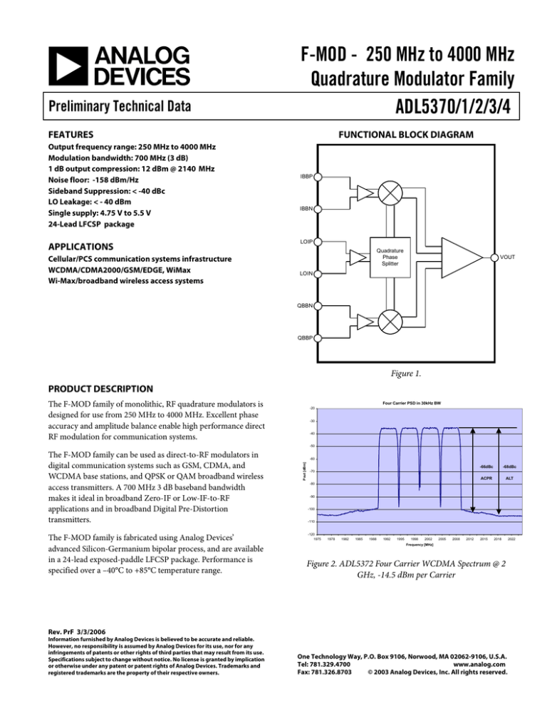
Figure 1.
PRODUCT DESCRIPTION
The F-MOD family of monolithic, RF quadrature modulators is
designed for use from 250 MHz to 4000 MHz. Excellent phase
accuracy and amplitude balance enable high performance direct
RF modulation for communication systems.
Four Carrier PSD in 30kHz BW
-20
-30
-40
-50
The F-MOD family is fabricated using Analog Devices’
advanced Silicon-Germanium bipolar process, and are available
in a 24-lead exposed-paddle LFCSP package. Performance is
specified over a –40°C to +85°C temperature range.
-60
Pout [dBm]
The F-MOD family can be used as direct-to-RF modulators in
digital communication systems such as GSM, CDMA, and
WCDMA base stations, and QPSK or QAM broadband wireless
access transmitters. A 700 MHz 3 dB baseband bandwidth
makes it ideal in broadband Zero-IF or Low-IF-to-RF
applications and in broadband Digital Pre-Distortion
transmitters.
-66dBc
-68dBc
ACPR
ALT
-70
-80
-90
-100
-110
-120
1975
1978
1982
1985
1988
1992
1995
1998
2002
2005
2008
2012
2015
2018
Frequency [MHz]
Figure 2. ADL5372 Four Carrier WCDMA Spectrum @ 2
GHz, -14.5 dBm per Carrier
Rev. PrF 3/3/2006
Information furnished by Analog Devices is believed to be accurate and reliable.
However, no responsibility is assumed by Analog Devices for its use, nor for any
infringements of patents or other rights of third parties that may result from its use.
Specifications subject to change without notice. No license is granted by implication
or otherwise under any patent or patent rights of Analog Devices. Trademarks and
registered trademarks are the property of their respective owners.
One Technology Way, P.O. Box 9106, Norwood, MA 02062-9106, U.S.A.
Tel: 781.329.4700
www.analog.com
Fax: 781.326.8703
© 2003 Analog Devices, Inc. All rights reserved.
2022
ADL5370/1/2/3/4
Preliminary Technical Data
SPECIFICATIONS
Table 1. VS = 5 V; Ambient Temperature (TA) = 25°C; LO = 0 dBm1; I/Q inputs = 1.4 V p-p differential sine waves in quadrature on
a 500 mV dc bias; baseband frequency = 1 MHz, unless otherwise noted.
Parameter
Operating Frequency Range
ADL5370
Operating Frequency Range
Output Power
Output P1 dB
Carrier Feedthrough
Sideband Suppression
Second Harmonic
Third Harmonic
Output IP3
Noise Floor
GSM
ADL5371
Operating Frequency Range
Output Power
Output P1 dB
Carrier Feedthrough
Sideband Suppression
Second Harmonic
Third Harmonic
Output IP3
Noise Floor
GSM
ADL5372
Operating Frequency Range
Output Power
Output P1 dB
Carrier Feedthrough
Sideband Suppression
Second Harmonic
Third Harmonic
Output IP3
Noise Floor
WCDMA
GSM
WCDMA ACPR
Conditions
Frequency Range covered by F-Mod family
Low Frequency
High Frequency
LO = 450 MHz
Range over which Uncompensated Sideband Suppression < -30 dBc
Low Frequency
High Frequency
VIQ=1.4V pp differential
POUT – (FLO + (2 × FBB)), POUT = 7 dBm
POUT – (FLO + (3 × FBB)), POUT = 7 dBm
F1BB = 3 MHz, F2BB = 4 MHz, POUT = -2 dBm per tone
Baseband inputs biased to 500 mV; PLO = +0 dBm
FLO = 380 MHz, 6 MHz carrier offset, POUT = +6 dBm, PLO = +3 dBm
LO = 900 MHz
Range over which Output P1dB > 10 dBm
Low Frequency
High Frequency
VIQ=1.4Vpp differential
POUT – (FLO + (2 × FBB)), POUT = 7 dBm
POUT – (FLO + (3 × FBB)), POUT = 7 dBm
F1BB = 3 MHz, F2BB = 4 MHz, POUT = -2 dBm per tone
Baseband inputs biased to 500 mV; PLO = +6 dBm
FLO = 885 MHz, 6 MHz carrier offset, POUT = +7 dBm, PLO = +6 dBm
LO = 1900 MHz, 2140 MHz
Range over which Output P1dB > 10 dBm
Low Frequency
High Frequency
VIQ=1.4Vpp differential
POUT – (FLO + (2 × FBB)), POUT = 7 dBm
POUT – (FLO + (3 × FBB)), POUT = 7 dBm
F1BB = 3 MHz, F2BB = 4 MHz, POUT = -2 dBm per tone
Baseband inputs biased to 500 mV; PLO = +6 dBm
Single Carrier WCDMA, 20 MHz Carrier Offset, Pout=-10 dBm, PLO= 0 dBm
FLO = 900 MHz, 6 MHz carrier offset, POUT = +9dBm, PLO = +6 dBm
Single Carrier, Test Model 1-64, Pout = -10 dBm, PLO = 0 dBm
Four Carrier, Test Model 1-64, Pout (total) = -10 dBm, PLO = 0 dBm
Rev. PrF | Page 2 of 11
Min
Typ
Max
Unit
MHz
250
4000
MHz
250
1300
5.6
10.5
-50
-42
-54
-50
24
-156
-154
MHz
MHz
dBm
dBm
dBm
dBc
dBc
dBc
dBm
dBm/Hz
dBc/Hz
700
1300
6.5
13
-40
-52
-50
-48
24
-156
-158
MHz
MHz
dBm
dBm
dBm
dBc
dBc
dBc
dBm
dBm/Hz
dBc/Hz
1600
2400
6
12
-37
-38
-45
-47
26
-158
-156
-158
-75
-65
MHz
MHz
dBm
dBm
dBm
dBc
dBc
dBc
dBm
dBm/Hz
dBm/Hz
dBc/Hz
dBc
dBc
Preliminary Technical Data
Parameter
ADL5373
Operating Frequency Range
Output Power
Output P1 dB
Carrier Feedthrough
Sideband Suppression
Second Harmonic
Third Harmonic
Output IP3
Noise Floor
ADL5374
Operating Frequency Range
Output Power
Output P1 dB
Carrier Feedthrough
Sideband Suppression
Second Harmonic
Third Harmonic
Output IP3
Noise Floor
LO INPUTS
LO Drive Level1
Nominal Impedance
Input Return Loss
BASEBAND INPUTS
I and Q Input Bias Level
Bandwidth (3 dB)
POWER SUPPLIES
Voltage
Supply Current
ADL5370/1/2/3/4
Conditions
LO = 2500 MHz
Min
Typ
Max
TBD
2500
6
TBD
-47
-33
-37
-42
TBD
TBD
TBD
3500
4.3
TBD
-42
-36
-31
-42
TBD
TBD
TBD
VIQ=1.4Vpp differential
POUT – (FLO + (2 × FBB)), POUT = 7 dBm
POUT – (FLO + (3 × FBB)), POUT = 7 dBm
F1BB = 3 MHz, F2BB = 4 MHz, POUT = -3 dBm per tone
Baseband inputs biased to 500 mV, PLO = +6 dBm
LO = 3500 MHz
TBD
VIQ=1.4Vpp differential
POUT – (FLO + (2 × FBB)), POUT = 7 dBm
POUT – (FLO + (3 × FBB)), POUT = 7 dBm
F1BB = 3 MHz, F2BB = 4 MHz, POUT = -3 dBm per tone
Baseband inputs biased to 500 mV, PLO = +6 dBm
Characterization performed at typical level
-3
0
50
Unit
dBm
dBm
dBm
dBc
dBc
dBc
dBm
dBm/Hz
-
3
-10
dBm
dBm
dBm
dBc
dBc
dBc
dBm
dBm/Hz
dBm
Ω
dB
Pins IBBP, IBBN, QBBP, QBBN
400
500
700
600
mV
MHz
5.5
V
Pins VPS1 and VPS2
4.75
ADL5370
ADL5371, ADL5372, ADL5373, ADL5374
210
175
Notes
1 LO drive in excess of +3 dBm can be provided to further reduce noise at 6 MHz and 20 MHz carrier offsets in GSM and WCDMA applications respectively.
Rev. PrF | Page 3 of 11
mA
ADL5370/1/2/3/4
Preliminary Technical Data
ABSOLUTE MAXIMUM RATINGS
Table 2. F-MOD Absolute Maximum Ratings
Parameter
Supply Voltage VPOS
IBBP, IBBN, QBBP, QBBN
LOIP and LOIN
Internal Power Dissipation
θJA (Exposed Paddle Soldered Down)
Maximum Junction Temperature
Operating Temperature Range
Storage Temperature Range
Rating
5.5 V
0 V, 2.5 V
10 dBm
800 mW
30°C/W
125°C
−40°C to +85°C
−65°C to +150°C
Stresses above those listed under Absolute Maximum Ratings
may cause permanent damage to the device. This is a stress
rating only; functional operation of the device at these or any
other conditions above those indicated in the operational
section of this specification is not implied. Exposure to absolute
maximum rating conditions for extended periods may affect
device reliability.
ESD CAUTION
ESD (electrostatic discharge) sensitive device. Electrostatic charges as high as 4000 V readily accumulate on
the human body and test equipment and can discharge without detection. Although this product features
proprietary ESD protection circuitry, permanent damage may occur on devices subjected to high energy
electrostatic discharges. Therefore, proper ESD precautions are recommended to avoid performance
degradation or loss of functionality.
Rev. PrF | Page 4 of 11
Preliminary Technical Data
ADL5370/1/2/3/4
IBBP 19
IBBN 20
COMM 21
COMM 22
QBBN 23
QBBP 24
PIN CONFIGURATION AND FUNCTIONAL DESCRIPTIONS
1 COMM
VPS5 18
2 COMM
VPS4 17
3 VPS1
VPS3 16
FMOD
4 VPS1
VPS2 15
VPS2 14
5 VPS1
Exposed Paddle
VOUT 13
6 VPS1
COMM 12
COMM 11
COMM 10
LOIN 9
LOIP 8
COMM 7
Figure 2.
Table 3. Pin Function Descriptions
Pin No.
1,2,7,10,11,12,21,22
3,4,5,6,14,15,16,17,18
Mnemonic
COMM
VPS1,VPS2,
VPS3,VPS4,VPS5
19,20,23,24
IBBP,IBBN,
QBBN,QBBP
8,9
LOIP, LOIN
13
VOUT
Exposed Paddle
Description
Input Common Pins. Connect to ground plan via a low impedance path
Positive Supply Voltage pins. All pins should be connected to the same supply. To ensure
adequate external bypassing, connect 0.1 μF capacitors between each pin and ground.
Adjacent power supply pins of the same name can share one capacitor (see evaluation
board schematic).
Differential In-Phase and Quadrature Baseband Inputs. These high impedance inputs must
be dc-biased to approximately 500 mV dc, and must be driven from a low impedance
source. Nominal characterized ac signal swing is 700 mV p-p on each pin. This results in a
differential drive of 1.4 V p-p with a 500 mV dc bias. These inputs are not self-biased and
must be externally biased.
50 Ω Single-Ended Local Oscillator Input. Internally dc-biased. Pins must be ac-coupled. ACcouple LOIN to ground and drive LO through LOIP.
Device Output. Single-ended, 50 Ω internally biased RF output. Pin must be ac-coupled to
the load.
Connect to ground plan via a low impedance path
Rev. PrF | Page 5 of 11
ADL5370/1/2/3/4
Preliminary Technical Data
Four Carrier PSD in 30kHz BW
Output Power vs. LO Frequency FMOD2
Temperature = {-40'C, 25'C, 85'C}; VPOS = 5.0V; VCM = 0.5V; BB Frequency = 1MHZ;
BB_AMP = 0.7 Vpp; LO POWER = -7 dBm
-20
-30
8
-40
7
-50
6
-66dBc
-68dBc
ACPR
ALT
-70
-80
-90
5
25'C
-40'C
4
85'C
3
2
-100
1
-110
-120
1975
Output Power (dBm)
Pout [dBm]
-60
1978
1982
1985
1988
1992
1995
1998
2002
2005
2008
2012
2015
2018
2022
0
1500
1600
1700
1800
1900
2000
2100
2200
2300
2400
2500
Output Freque ncy (MHz)
Frequency [MHz]
Figure 3. ADL5372 Four Carrier WCDMA Spectrum (Test Model
1-64) @ 2 GHz, -14.5 dBm per Carrier, ACPR = -66 dBc, Zero IF
Figure 6. ADL5372 Output Power vs. Frequency and Temperature.
Baseband drive is 1.4 Vpp differential
Figure 4. ADL5372 Two Carrier WCDMA Spectrum(Test Model
1-64) (Test Model 1-64) @ 2.1 GHz, -11.7 dBm per Carrier,
ACPR = -69 dBc, Baseband drive from AD9779 Dual DAC at 96
MHz
Figure 7. ADL5372 WCDMA Single Carrier 64-Users ACPR versus
Output Power at 2140 MHz, Plo=+3dBm, Zero IF
-145.00
-150.00
Noise (dBc/Hz)
6 MHz offset
-155.00
-160.00
-165.00
-10
-5
0
Plo (dBm)
5
10
Figure 5. ADL5371 GSM Noise at 900 MHz vs. LO Drive, 6 MHz
Carrier Offset. Pout = +5 dBm
Figure 4. ADL5372 Single Carrier WCDMA Noise at 1.96 GHz, 50MHz carrier offset,Test Model 1-64, Zero IF
Rev. PrF | Page 6 of 11
Preliminary Technical Data
ADL5370/1/2/3/4
Carried Feedthrough vs. LO Frequency FMOD0 with Carrier Nulling applied at 25'C
Temperature = {-40'C, 25'C, 85'C}; VPOS = 5.0V; VCM = 0.5V; BB Frequency = 1MHZ;
LO POWER = -7 dBm
0
0
-10
-10
-20
-20
Carrierfeedthrough (dBm)
Carrierfeedthrough (dBm)
Carried Feedthrough vs. LO Frequency FMOD0
Temperature = {-40'C, 25'C, 85'C}; VPOS = 5.0V; VCM = 0.5V; BB Frequency = 1MHZ;
LO POWER = -7 dBm
-30
-40
-50
-60
25'C
-40'C
-40
85'C
-50
-60
-70
25'C
-70
-30
-40'C
85'C
-80
-80
-90
-90
0
200
400
600
800
1000
1200
1400
0
1600
200
400
600
800
1000
1200
1400
1600
Output Frequency (MHz)
Output Frequency (MHz)
Figure 9. ADL5370 Uncalibrated Carrier Feed through
Figure 12. ADL5370 Carrier Feed through with Nulling at 25C
Undesired Side Band vs. LO Frequency FMOD0
Temperature = {-40'C, 25'C, 85'C}; VPOS = 5.0V; VCM = 0.5V; BB Frequency = 1MHZ;
LO POWER = -7 dBm
Undesired Side Band vs. LO Frequency FMOD0
with NULLING applied at 25'C
Temperature = {-40'C, 25'C, 85'C}; VPOS = 5.0V; VCM = 0.5V; BB Frequency = 1MHZ;
BB_AMP = 0.7Vpp; LO POWER = -7 dBm
0
0
-10
-10
-20
Sideband Suppression (dBc)
Sideband Suppression (dBc)
-20
25'c
-30
-40'c
85'c
-40
-50
-60
-30
25'C
-40'C
-40
85'C
-50
-60
-70
-70
-80
-80
-90
-90
50
50
250
450
650
850
1050
1250
250
450
650
1450
850
1050
1250
1450
Output Frequency (MHz)
Output Fre quency (MHz)
Figure 10. ADL5370 Uncalibrated Undesired Side band
Figure 13. ADL5370 Undesired Sideband with Nulling at 25C
Carried Feedthrough vs. LO Frequency FMOD1
Temperature = {-40'C, 25'C, 85'C}; VPOS = 5.0V; VCM = 0.5V; BB Frequency = 1MHZ;
LO POWER = -7 dBm
Carried Feedthrough vs. LO Frequency FMOD1
with Nulling applied at 25'C
Temperature = {-40'C, 25'C, 85'C}; VPOS = 5.0V; VCM = 0.5V; BB Frequency = 1MHZ;
LO POWER = -7 dBm
0
10
-10
0
-20
-10
-30
-20
25'c
-40'c
-40
116_-7_0.7
116_-7_0.7
116_-7_0.7
-50
-60
Carrierfeedthrough (dBm )
Carrierfeedthrough (dBm)
85'c
-30
-40
-50
-60
-70
-70
-80
-80
-90
-90
500
600
700
800
900
1000
1100
1200
1300
1400
500
1500
600
700
800
900
1000
1100
1200
1300
1400
1500
Output Frequency (MHz)
Output Frequency (MHz)
Figure 11. ADL5371 Uncalibrated Carrier Feed through
Figure 14. ADL5371 Carrier Feed through with Nulling at 25C
Rev. PrF | Page 7 of 11
ADL5370/1/2/3/4
Preliminary Technical Data
Undesired Side Band vs. LO Frequency FMOD1
Temperature = {-40'C, 25'C, 85'C}; VPOS = 5.0V; VCM = 0.5V; BB Frequency = 1MHZ;
LO POWER = -7 dBm
Undesired Side Band vs. LO Frequency FMOD1
Temperature = {-40'C, 25'C, 85'C}; VPOS = 5.0V; VCM = 0.5V; BB Frequency = 1MHZ;
LO POWER = -7 dBm
0
0
-10
-10
-20
-30
-40
116_-7_0.7
116_-7_0.7
116_-7_0.7
-50
Sideband Suppression (dBc)
Sideband Suppression (dBc)
-20
-30
-40
139_-7_0.699999988079071
139_-7_0.699999988079071
139_-7_0.699999988079071
-50
-60
-60
-70
-70
-80
-80
-90
500
600
700
800
-90
900
1000
1100
1200
1300
1400
1500
Output Freque ncy (MHz)
500
600
700
800
900
1000
1100
1200
1300
1400
1500
Output Frequency (MHz)
Figure 15. ADL5371 Uncalibrated Undesired Side band
Figure 18. ADL5371 Undesired Sideband with Nulling at 25C
Carried Feedthrough vs. LO Frequency FMOD2
Temperature = {-40'C, 25'C, 85'C}; VPOS = 5.0V; VCM = 0.5V; BB Frequency = 1MHZ;
BB_AMP = 0.7 Vpp; LO POWER = -7 dBm
0
Carrierfeedthrough (dBm)
-10
-20
25'C
-30
-40'C
85'C
-40
-50
-60
1500
1600
1700
1800
1900
2000
2100
2200
2300
2400
2500
Output Freque ncy (MHz)
Figure 16. ADL5372 Uncalibrated Carrier Feed through
Figure 19. ADL5372 Carrier Feed through with Nulling at 25C
Undesired Side Band vs. LO Frequency FMOD2
Temperature = {-40'C, 25'C, 85'C}; VPOS = 5.0V; VCM = 0.5V; BB Frequency = 1MHZ;
LO POWER = -7 dBm
Undesired Side Band vs. LO Frequency FMOD2
With Nulling Applied at 25'C
Temperature = {-40'C, 25'C, 85'C}; VPOS = 5.0V; VCM = 0.5V; BB Frequency = 1MHZ;
LO POWER = -7 dBm
0
0
-10
-10
-20
-30
25
-40
-40
85
-50
Sideband Suppression (dBc)
Sideband Suppression (dBc)
-20
-30
25'C
-40
-40'C
85'C
-50
-60
-60
-70
-70
-80
1500
1600
1700
1800
1900
2000
2100
2200
2300
2400
2500
-80
1500
Figure 17. ADL5372 Uncalibrated Undesired Side band
1600
1700
1800
1900
2000
2100
2200
2300
2400
2500
Output Frequency (MHz)
Output Fre quency (MHz)
Figure 20. ADL5372 Undesired Sideband with Nulling at 25C
Rev. PrF | Page 8 of 11
Preliminary Technical Data
ADL5370/1/2/3/4
BASIC CONNECTIONS
performance.
Refer to the evaluation board schematic for the basic
connections for operating the F-MOD family.
The baseband inputs QBBP, QBBN, IBBP and IBBN must be
driven from a differential source. The nominal drive level of 1.4
Vpp differential (700 mVpp on each pin) should be biased at
500 mV.
A single power supply of between 4.75 V and 5.5 V is applied to
pins VPS1 and VPS2 and VPS3. All the VPS pins must be
connected to the same potential. Adjacent pins of the same
name can be tied together and decoupled with a 0.1 uF
capacitor. These capacitors should be located as close as possible
to the device.
A Single–ended Local Oscillator signal should be applied to the
LOIP pin through an ac-coupling capacitor. The recommended
LO drive power is 0 dBm. The LO return pin, LOIN, should be
ac-coupled to ground though a low impedance path.
All the COMM pins should be tied to the same ground plane
through low impedance paths. The exposed paddle on the
under side of the package should also be soldered to a low
impedance ground plane. If multiple ground planes exist on the
circuit board, these should be stitched together with multiple
(typically 9) vias to enhance thermal and electrical
RFPQ
0Ω
RFNQ
0Ω
RFNI
0Ω
CFNQ
Open
CFNI
Open
ENBL
SW21
RFPI
0Ω
RTI
Open
VPS5 18
2 COMM
VPS4 17
Z1
ENBL
3 VPS1
R22
10k
VPS2 15
L11
0
VPOS
VOUT 13
6 VPS1
COMM 12
COMM 11
COMM 10
CLOP
100pF
LOIN 9
LOIP 8
COMM 7
GND
C14
0.1uF
C13
0.1uF
Exposed Paddle
C12
0.1uF
L12
0
VPS2 14
5 VPS1
VPOS
C15
0.1uF
VPS3 16
FMOD
4 VPS1
VPOS
C16
0.1uF
1 COMM
OFF
R21
49.9
CFPI
Open
IBBP 19
QBBN 23
QBBP 24
RTQ
Open
IBBP
IBBN 20
IBBN
COMM 21
QBBN
COMM 22
QBBP
CFPQ
Open
ON
The RF output is available at the VOUT pin (Pin 7). This pin
must also be ac-coupled. Both LOIP and VOUT have nominal
broadband input and output impedances of 50 Ω and do not
need further external matching.
COUT
100pF
CLON
100pF
LO
Figure 5. F-MOD Evaluation Board Schematic.
Rev. PrF | Page 9 of 11
C11
OPEN
VOUT
ADL5370/1/2/3/4
Preliminary Technical Data
EVALUATION BOARD
Populated RoHS-compliant evaluation boards are available for
the F-MOD family (see Ordering Guide for evaluation board
part numbers). Each device has an exposed paddle underneath
the package, which must be soldered to the board. The
evaluation board is designed without any components on the
underside of the board so that heat may be applied to the
underside for easy removal and replacement of the F-MOD.
Note that the evaluation board pcb design includes an Enable
Output SMA connector (ENOP) and switch (SW21) which
connect ground or supply to pin 3. Since the F-MOD family
does not support the Enable Output function (pin 3 is a power
supply pin), SW21 should be placed in the ON position. This
connects pin 3 to supply.
Figure 6. Evaluation Board Layout, Top Layer.
Table 4. Evaluation Board Configuration Options
Component
VPOS, GND
SW21, ENOP SMA Connector
RFPI,RFNI,RFPQ,RFNQ,
CFPI, CFNI, CFPQ,CFNQ,
RTQ, RTI,
Function
Power Supply and Ground Clip Leads
Enable Output Function (not supported in F-Mod family)
Baseband Input Filters: These components can be used
to implement a low-pass filter for the baseband signals.
Rev. PrF | Page 10 of 11
Default Condition
Not applicable
SW21 = ON (connects pin 3 (VPS1) to supply)
RFNQ, RFPQ, RFNI RFPI = 0 Ω (0402)
CFNQ,CFPQ,CFNI,CFPI = Open (0402)
RTQ, RTI = Open (0402)
Preliminary Technical Data
ADL5370/1/2/3/4
OUTLINE DIMENSIONS
Figure 7. 24-Lead LFCSP with exposed paddle. Dimensions shown in millimeters
ORDERING GUIDE
Model
ADL5370ACPZ-R71
ADL5370ACPZ-WP1
ADL5370-EVALZ1
ADL5371ACPZ-R71
ADL5371ACPZ-WP1
ADL5371-EVALZ1
ADL5372ACPZ-R71
ADL5372ACPZ-WP1
ADL5372-EVALZ1
ADL5373ACPZ-R71
ADL5373ACPZ-WP1
ADL5373-EVALZ1
ADL5374ACPZ-R71
ADL5374ACPZ-WP1
ADL5374-EVALZ1
ADL5375ACPZ-R71
ADL5375ACPZ-WP1
ADL5375-EVALZ1
1
Temperature Range (°C)
–40 to +85
–40 to +85
–40 to +85
–40 to +85
–40 to +85
–40 to +85
–40 to +85
–40 to +85
–40 to +85
–40 to +85
–40 to +85
–40 to +85
Package Description
7" Tape and Reel
Waffle Pack
Evaluation Board
7" Tape and Reel
Waffle Pack
Evaluation Board
7" Tape and Reel
Waffle Pack
Evaluation Board
7" Tape and Reel
Waffle Pack
Evaluation Board
7" Tape and Reel
Waffle Pack
Evaluation Board
7" Tape and Reel
Waffle Pack
Evaluation Board
Z indicates Pb-free
Rev. PrF | Page 11 of 11
Package Option

![dB = 10 log10 (P2/P1) dB = 20 log10 (V2/V1). dBm = 10 log (P [mW])](http://s2.studylib.net/store/data/018029789_1-223540e33bb385779125528ba7e80596-300x300.png)
