as a PDF
advertisement

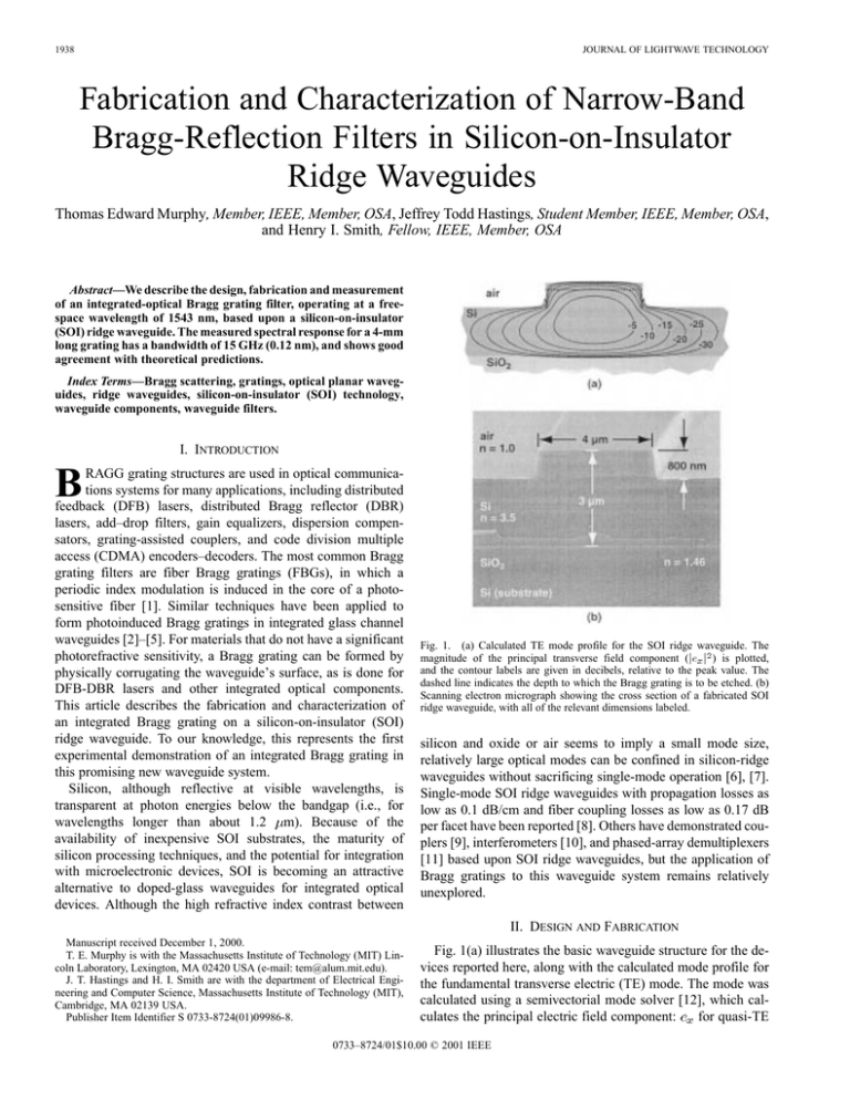
1938 JOURNAL OF LIGHTWAVE TECHNOLOGY Fabrication and Characterization of Narrow-Band Bragg-Reflection Filters in Silicon-on-Insulator Ridge Waveguides Thomas Edward Murphy, Member, IEEE, Member, OSA, Jeffrey Todd Hastings, Student Member, IEEE, Member, OSA, and Henry I. Smith, Fellow, IEEE, Member, OSA Abstract—We describe the design, fabrication and measurement of an integrated-optical Bragg grating filter, operating at a freespace wavelength of 1543 nm, based upon a silicon-on-insulator (SOI) ridge waveguide. The measured spectral response for a 4-mm long grating has a bandwidth of 15 GHz (0.12 nm), and shows good agreement with theoretical predictions. Index Terms—Bragg scattering, gratings, optical planar waveguides, ridge waveguides, silicon-on-insulator (SOI) technology, waveguide components, waveguide filters. I. INTRODUCTION B RAGG grating structures are used in optical communications systems for many applications, including distributed feedback (DFB) lasers, distributed Bragg reflector (DBR) lasers, add–drop filters, gain equalizers, dispersion compensators, grating-assisted couplers, and code division multiple access (CDMA) encoders–decoders. The most common Bragg grating filters are fiber Bragg gratings (FBGs), in which a periodic index modulation is induced in the core of a photosensitive fiber [1]. Similar techniques have been applied to form photoinduced Bragg gratings in integrated glass channel waveguides [2]–[5]. For materials that do not have a significant photorefractive sensitivity, a Bragg grating can be formed by physically corrugating the waveguide’s surface, as is done for DFB-DBR lasers and other integrated optical components. This article describes the fabrication and characterization of an integrated Bragg grating on a silicon-on-insulator (SOI) ridge waveguide. To our knowledge, this represents the first experimental demonstration of an integrated Bragg grating in this promising new waveguide system. Silicon, although reflective at visible wavelengths, is transparent at photon energies below the bandgap (i.e., for wavelengths longer than about 1.2 m). Because of the availability of inexpensive SOI substrates, the maturity of silicon processing techniques, and the potential for integration with microelectronic devices, SOI is becoming an attractive alternative to doped-glass waveguides for integrated optical devices. Although the high refractive index contrast between Fig. 1. (a) Calculated TE mode profile for the SOI ridge waveguide. The magnitude of the principal transverse field component (je j ) is plotted, and the contour labels are given in decibels, relative to the peak value. The dashed line indicates the depth to which the Bragg grating is to be etched. (b) Scanning electron micrograph showing the cross section of a fabricated SOI ridge waveguide, with all of the relevant dimensions labeled. silicon and oxide or air seems to imply a small mode size, relatively large optical modes can be confined in silicon-ridge waveguides without sacrificing single-mode operation [6], [7]. Single-mode SOI ridge waveguides with propagation losses as low as 0.1 dB/cm and fiber coupling losses as low as 0.17 dB per facet have been reported [8]. Others have demonstrated couplers [9], interferometers [10], and phased-array demultiplexers [11] based upon SOI ridge waveguides, but the application of Bragg gratings to this waveguide system remains relatively unexplored. II. DESIGN AND FABRICATION Manuscript received December 1, 2000. T. E. Murphy is with the Massachusetts Institute of Technology (MIT) Lincoln Laboratory, Lexington, MA 02420 USA (e-mail: tem@alum.mit.edu). J. T. Hastings and H. I. Smith are with the department of Electrical Engineering and Computer Science, Massachusetts Institute of Technology (MIT), Cambridge, MA 02139 USA. Publisher Item Identifier S 0733-8724(01)09986-8. Fig. 1(a) illustrates the basic waveguide structure for the devices reported here, along with the calculated mode profile for the fundamental transverse electric (TE) mode. The mode was calculated using a semivectorial mode solver [12], which calfor quasi-TE culates the principal electric field component: 0733–8724/01$10.00 © 2001 IEEE MURPHY et al.: NARROW-BAND BRAGG-REFLECTION FILTERS modes and for quasi-TM modes. In Fig. 1(a), is plotted and the contour labels are given in decibels, relative to the peak value. The composition and cross-sectional dimensions of the waveguides are indicated in the micrograph shown in Fig. 1(b). The full silicon layer thickness is 3 m, and the ridge is etched to a depth of 800 nm. The Bragg grating is etched into the top of the ridge, to a depth of 150 nm. By choosing the ridge height to be somewhat less than the full silicon layer height, single-mode operation is ensured. For a first-order Bragg grating operating at a free-space wavelength of 1550 nm, the required Bragg grating period is about 223 nm. For the devices reported here, the duty cycle (the fraction of the period occupied by a grating tooth) was close to 50%. The effect of the grating can be modeled using coupled-mode theory (CMT), in which the grating coupling strength (usually denoted by ) is described by a simple overlap integral between the optical waveguide mode and the grating region [13], [14]. From a lithography standpoint, it is difficult to form a submicron pitch grating with an aspect ratio much larger than 2:1, which corresponds to a maximum grating depth of about 200 nm for silicon ridge waveguides. Moreover, theoretical models predict that little is gained by making the grating much deeper than the exponential decay length (or skin depth) of the electromagnetic mode. With these limitations in mind, we chose the grating depth to be 150 nm. For a fixed grating depth, the grating strength ( ) depends upon the waveguide dimensions. The waveguide structure shown in Fig. 1 was selected as a compromise between two extremes. For ridge waveguides designed to match well to an optical fiber (i.e., when the silicon thickness is about 5–7 m), a relatively shallow grating atop the ridge would constitute a very weak perturbation, and would not be suitable for most integrated filter applications. At the other extreme, for single-mode channel waveguides in silicon (e.g., when the silicon layer is only 100–200 nm thick), the grating is strong enough to be considered a one-dimensional photonic bandgap structure [15]. However, such submicron silicon waveguides often have unacceptably high propagation loss and inefficient coupling to an optical fiber. The intermediate structure shown in Fig. 1 offers reasonable grating strength with a relatively large mode size. The raw materials used for this work were commercially available ELTRAN SOI wafers (Canon, Inc., Hiratsuka-shi, Kanagawa, Japan). The supplier used a sequence of silicon epitaxy, flip bonding, and selective back etching to generate SOI wafers with an oxide thickness of 1 m and a silicon thickness of 3 m [16], [17]. Fig. 2 outlines the lithographic sequence we implemented to pattern the fine-period Bragg gratings on top of silicon ridge waveguides. We earlier reported using a similar process for InP waveguide fabrication [18]. First, a uniform layer of is deposited over the silicon core layer via -beam evaporation of SiO , and patterned using interference lithography and reactive ion etching (RIE) in CHF . This oxide grating pattern will later serve as a mask for etching the Bragg gratings. The comparatively coarse waveguide features are patterned in nickel directly on top of the oxide grating using scanning electron-beam lithography and a liftoff process. After the gratings and waveguides have been patterned, the device is 1939 Fig. 2. Fabrication process used to pattern the fine-period Bragg gratings on top of SOI ridge waveguides. Two masking layers are first patterned, one on top of the other, to define the gratings and the waveguides. The device is then formed through a sequence of selective etching steps. Fig. 3. Scanning-electron micrograph showing a silicon-on-insulator ridge waveguide with a 223-nm period Bragg grating patterned on the top surface. formed by a sequence of selective etching steps as shown in Fig. 2(c)–(f). The excess grating is first removed using RIE in a CHF plasma. Next, the waveguide is formed using RIE in a CF –O plasma. After stripping the nickel waveguide mask, the gratings are etched to a depth of 150 nm in a Cl plasma. The oxide-masking layer is then removed, completing the process. Fig. 3 is a micrograph showing a completed device with a 223-nm period Bragg grating patterned on a ridge waveguide. The first benefit of this process is that the most critical nanolithography step (that in which the Bragg gratings are formed) is performed over a planar surface. Because the initial grating pattern can be made relatively thin, the second level of lithography, likewise, has very little surface topography to contend with. A second benefit is that the gratings can be made wider than the waveguides, allowing for relaxed tolerance when placing the 1940 JOURNAL OF LIGHTWAVE TECHNOLOGY Fig. 5. Measured TE transmission spectrum for the Bragg gratings. The first three dips in transmission are identified with coupling to leaky modes, whereas the final dip at 1543 nm is the anticipated coupling into the backward-traveling bound mode. Fig. 4. (a) Top-down diagram illustrating the layout of the Bragg grating devices. The grating length was 4 mm, and the full chip length was 17 mm. The waveguides were bent to an angle of 6 at the chip facets to eliminate unwanted reflections. (b) Illustration of the system used to measure the devices. Light was coupled into the waveguides using a lensed fiber and collected at the output with a microscope objective. Notice that the sample must be rotated by 21 in order to account for refraction at the input and output facets. waveguides. When the excess grating to either side of the waveguide is stripped, the remaining grating lines are automatically confined to the tops of the waveguides. Fig. 4(a) is a top-down diagram illustrating the layout of the devices that we measured. The gratings were 4-mm long and the full chip length was 17 mm. The waveguides were bent to an angle of 6 at the edges of the chip to eliminate internal reflections from the facets. The bending radius was 15 mm, which was predicted to yield negligible bending loss for the waveguides considered. III. MEASUREMENT Light from a tunable external-cavity diode laser was coupled into the device using a conical lensed fiber and collected from the output facet using a microscope objective, as shown in Fig. 4(b). Notice that the entire chip must be rotated by about 21 to account for refraction of the light as it enters and exits the device. The laser output was connected through a polarization controller (not depicted) before entering the chip, and a linear polarizer was inserted after the microscope objective to analyze the polarization of the light emerging from the chip. For each measurement, the polarization controller was adjusted until the emerging light was linearly polarized in either the TE or TM state. Prior to measuring the devices, the output of the lensed fiber was focused through the objective lens directly onto the detector in order to quantify the relative amount of light entering the device. After the device was inserted and all the elements aligned, the detected power decreased by 12.3 dB for the TE polarization and 13.6 dB for the TM polarization. These insertion loss figures include mode mismatch at the input facet, waveguide propagation loss, possible grating-induced loss, Fresnel reflection at both facets, and bending loss. The theoretically calculated Fresnel reflection loss is 2.9 dB for TE and 3.5 dB for TM. When the same procedure is applied to a similar waveguide without Bragg gratings, the measured insertion loss remains unchanged, indicating that the grating-induced excess loss is not appreciable. The remaining 10 dB of loss is thought to be due mostly to waveguide propagation loss, with a small component attributable to input mode mismatch. We believe that the propagation loss is primarily caused by roughness and irregularities in the side walls of the waveguide which arise during lithographic processing, and we anticipate that improvements to the fabrication sequence will lead to lower propagation loss [19]. Fig. 5 depicts the measured transmission spectrum for a 4-mm long Bragg grating. A similar spectrum is seen for the TM polarization. The transmission spectrum shows four distinct dips, and more might be present at shorter wavelengths that our laser could not reach. The first three dips at 1510 nm, 1525 nm, and 1537 nm can be identified with grating-assisted coupling between the forward-traveling bound mode and backward-traveling leaky modes, whereas the final dip at 1543 nm corresponds to the anticipated coupling from the forward to the backward guided mode. Even though the waveguide under consideration only supports one bound mode per polarization state, there are several leaky modes associated with higher order slab modes of the structure. The physical mechanism of the leaky mode coupling can be understood by considering a simplified model of the system consisting of a three-layer slab waveguide, depicted in Fig. 6(a). The dimensions of the slab waveguide have been chosen to correspond to the full height of the silicon guiding layer in the real devices. Even though the ridge structure has only one bound mode, the slab waveguide has multiple modes. Although the ridge structure provides confinement in the transverse direction for the fundamental mode, the higher-order MURPHY et al.: NARROW-BAND BRAGG-REFLECTION FILTERS 1941 Fig. 7. Enlarged plot of the measured transmission spectrum of the Bragg grating around 1543 nm, showing both polarizations. The TM spectrum has been offset by 2 dB to differentiate the two. The dashed lines represent the theoretically calculated spectrum, obtained from CMT. 0 Fig. 6. (a) A simple three-layer slab waveguide model can be used to understand the observed Bragg transmission spectrum. As shown here, the dimensions of the slab waveguide were chosen to be similar to the ridge waveguide which we actually measured. (b) The calculated dispersion relation ( vs ) for the first four modes of the slab waveguide depicted in (a). The corresponding backward-traveling modes (with negative ) are also plotted. When a Bragg grating is introduced, coupling can occur wherever the difference in propagation constants matches the spatial frequency (k vector) of the Bragg grating. The four vertical arrows in this figure indicate the four wavelengths at which light from the forward-traveling fundamental mode can couple to one of the four backward-traveling modes. modes leak out of the waveguide to either side of the ridge. Thus, we can associate the higher order slab modes with leaky modes. Fig. 6(b) plots the calculated dispersion relation ( versus ) for the first four TE modes of the slab waveguide depicted in Fig. 6(a). Notice that we have also plotted the negative propagation constants, which correspond to the lowest four backward-traveling modes. The Bragg grating creates a coupling between the modes wherever the difference between their propagation constants is equal to the vector of the grating as follows: (1) where is the period of the Bragg grating. The four arrows drawn in Fig. 6(b) all of have the same length, and they illustrate the four wavelengths at which light from the forward-traveling fundamental mode can couple to one of the backward-traveling modes. The position and relative spacing of these four wavelengths agrees qualitatively with the measured data presented in Fig. 5, in spite of the simplifying approximations made (i.e., replacing the ridge with a slab). Fig. 7 shows an enlarged plot of the Bragg transmission spectrum around 1543 nm. Both TE and TM measurements are included in this plot, and the TM spectrum has been offset by dB to more clearly differentiate the two. CMT predicts that the peak reflectivity of a Bragg grating is (2) is the grating length and is the grating strength. where Using this relation, it is possible to infer the grating strength from the depth of the measured transmission spectrum and the known grating length. For the TE transmission spectrum, we observe a peak reflectivity of 90%, and infer a grating strength of cm . This figure agrees well with that predicted by the overlap integral method in conjunction with a semivectorial eigenmode solver [12]. For the TM polarization, the observed peak reflectivity is 50% and the grating strength is 2.1 cm , which is about 40% lower than that predicted by the overlap integral method. A more complete full-vector treatment might be needed to accurately model the Bragg reflection for the TM case. The dashed lines in Fig. 7 plot the calculated spectral response from CMT, showing the good agreement between theory and measurements. The spectral width at half maximum of the device is about 15 GHz, or 0.12 nm, for both polarizations. The TE and TM peaks are separated by 0.40 nm, and the theoretically predicted modal birefringence of the structure is 0.35 nm. These results suggest that modal birefringence (and not intrinsic material birefringence) is the dominant source of birefringence for the device. IV. CONCLUSION In this paper, we describe a fabrication process for building integrated Bragg gratings on SOI ridge waveguides, and we present our initial measurements of these devices. Our observations show that a nominally single-mode ridge waveguide can have higher-order leaky modes, which lead to loss on the blue side of the spectrum when the grating is measured in transmission. This effect is similar to the coupling to cladding modes that 1942 JOURNAL OF LIGHTWAVE TECHNOLOGY occurs in FBGs [20]. It should be possible to increase the spectral separation of these leaky modes by shrinking the waveguide dimensions, at the expense of reduced fiber coupling efficiency. Further study is needed to quantify the leaky mode spectrum for this class of waveguide. The primary Bragg transmission spectrum for a 4-mm long grating showed a spectral width of 15 GHz (0.12 nm) at 1543 nm, and peak reflectivity of 50% and 90% for TM and TE polarizations, respectively. Higher reflectivities could be achieved by increasing the grating length. The measurements show good agreement with theoretical models based on CMT. Although the devices here were designed for operation near 1550 nm, the technology could be used at wavelengths down to about 1.2 m by changing the grating pitch. ACKNOWLEDGMENT The authors would like to acknowledge Mark K. Mondol and Mike H. Lim for assistance in fabricating the devices. REFERENCES [1] A. Othonos, “Fiber Bragg gratings,” Rev. Sci. Instrum., vol. 68, no. 12, pp. 4309–4341, 1997. [2] G. D. Maxwell, R. Kashyap, B. J. Ainslie, D. L. Williams, and J. R. Armitage, “UV written 1.5 m reflection filters in single mode planar silica guides,” Electron. Lett., vol. 28, pp. 2106–2107, Oct. 22, 1992. [3] R. Kashyap, G. D. Maxwell, and B. J. Ainslie, “Laser-trimmed four-port bandpass filter fabricated in single-mode photosensitive germanium-doped planar waveguide,” IEEE Photon. Technol. Lett., vol. 5, pp. 191–194, Feb. 1993. [4] T. A. Strasser, T. Erdogan, A. E. White, V. Mizrahi, and P. J. Lamaire, “Ultraviolet laser fabrication of strong, nearly polarization-independent Bragg reflectors in germanium-doped silica waveguides on silica substrates,” Appl. Phys. Lett., vol. 65, no. 26, pp. 3308–3310, 1994. [5] G. E. Kohnke, C. H. Henry, E. J. Laskowski, M. A. Capuzzo, T. A. Strasser, and A. E. White, “Silica based mach-zehnder add-drop filter fabricated with UV induced gratings,” Electron. Lett., vol. 32, pp. 1579–1580, Aug. 17, 1996. [6] J. Schmidtchen, A. Splett, B. Schüppert, and K. Petermann, “Low loss single mode optical waveguides with large cross-section in silicon-oninsulator,” Electron. Lett., vol. 27, pp. 1486–1488, Aug. 1, 1991. [7] R. A. Soref, J. Schmidtchen, and K. Peterman, “Large single-mode rib waveguides in GeSi-Si and Si-on-SiO ,” J. Quantum Electron., pp. 1971–1973, Aug. 1991. [8] U. Fischer, T. Zinke, J.-R. Kropp, F. Arndt, and K. Peterman, “0.1 dB/cm waveguide losses in single-mode SOI rib waveguides,” IEEE Photon. Technol. Lett., vol. 8, pp. 647–648, May 1996. [9] P. D. Trinh, S. Yegnanarayanan, and B. Jalali, “Integrated optical directional couplers in silicon-on-insulator,” Electron. Lett., vol. 31, pp. 2097–2098, Nov. 23, 1995. [10] G. V. Treyz, “Silicon mach-zehnder waveguide interferometers operating at 1.3 ,” Electron Letters, vol. 27, pp. 118–120, Jan. 17, 1991. [11] P. D. Trinh, S. Yegnanarayanan, F. Coppinger, and B. Jalali, “Silicon-oninsulator (SOI) phased-array wavelength multi/demultiplexer with extremely low polarization sensitivity,” IEEE Photon. Technol. Lett., vol. 9, pp. 940–942, July 1997. [12] M. S. Stern, “Semivectorial polarized finite difference method for optical waveguides with arbitrary index profiles,” IEE Proc. Opt., vol. 135, no. 1, pp. 56–63, 1988. [13] A. Yariv and M. Nakamura, “Periodic structures for integrated optics,” J. Quantum Electron., vol. QE-13, no. 4, pp. 233–253, 1977. [14] B. E. Little and H. A. Haus, “A variational coupled-mode theory for periodic waveguides,” J. Quantum Electron., vol. 31, pp. 2258–2264, Dec. 1995. [15] J. S. Foresi, P. R. Villeneuve, J. Ferrera, E. R. Thoen, G. Steinmeyer, S. Fan, J. D. Joannopoulos, L. C. Kimerling, H. I. Smith, and E. P. Ippen, “Photonic-band-gap waveguide microcavities,” Nature, vol. 390, pp. 143–145, 1997. [16] T. Yonehara, K. Sakaguchi, and N. Sato, “Epitaxial layer transfer by bond and etch back of porous Si,” Appl. Phys. Lett., vol. 64, no. 16, pp. 2108–2110, 1994. [17] N. Sato and T. Yonehara, “Hydrogen annealed silicon-on-insulator,” Appl. Phys. Lett., vol. 65, no. 15, pp. 1924–1926, 1994. [18] M. H. Lim, T. E. Murphy, J. Ferrera, J. N. Damask, and H. I. Smith, “Fabrication techniques for grating-based optical devices,” J. Vac. Sci. Technol. B, vol. 17, no. 6, pp. 3208–3211, 1999. [19] K. K. Lee, D. R. Lim, H.-C. Luan, A. Agarwal, F. Foresi, and L. C. Kimerling, “Effect of size and roughness on light transmission in a Si/SiO waveguide: Experiments and model,” Appl. Phys. Lett., vol. 77, no. 11, pp. 1617–1619, 2000. [20] B. J. Eggleton, P. S. Westbrook, C. A. White, C. Kerbage, R. S. Windeler, and G. L. Burdge, “Cladding-mode resonances in air-silica microstructured optical fibers,” J. Lightwave Technol., vol. 18, pp. 1084–1100, Aug. 2000. Thomas Edward Murphy (M’98) was born in Falls Church, VA, in 1972. He received joint B.A. and B.S.E.E. degrees (summa cum laude) in physics and electrical engineering from Rice University, Houston, TX, in 1994, and the S.M. and Ph.D. degrees from the Massachusetts Institute of Technology (MIT), Cambridge, in 1997 and 2001, respectively. He joined the NanoStructures Laboratory at MIT in 1994, pursuing research in integrated optics and nanotechnology. In 2000, he joined the MIT Lincoln Laboratory, Lexington, MA, as a Staff Member in the Optical Communications Technology Group, where he is now actively involved in investigating and developing ultrafast optical communications systems. His research interests include optical communications, short-pulse phenomena, numerical simulation, transmission experiments, and integrated optics. Dr. Murphy is a member of the Optical Society of America (OSA), Tau Beta Pi, and Sigma Xi. In 1994, he was awarded a National Science Foundation fellowship for graduate research, and in 2000, he and his colleagues received the Lemelson-MIT student team prize for innovation in telecommunications and networking. Jeffrey Todd Hastings (S’98) received the B.S. degree in physics from Centre College, Danville, KY, in 1996 and the M.S. degree in electrical engineering from Purdue University, West Lafayette, IN, in 1998. He is working towards the Ph.D. degree in the Department of Electrical Engineering and Computer Science at the Massachusetts Institute of Technology, Cambridge. His research has encompassed novel designs and fabrication techniques for high speed high-efficiency light-emitting diodes, integrated optical devices, and semiconductor electronics. Mr. Hastings is a member of the Optical Society of America (OSA). Henry I. Smith (M’76–SM’84–F’87) holds the Joseph F. and Nancy P. Keithley Chair in Electrical Engineering at the Massachusetts Institute of Technology (MIT), Cambridge, and is Director of the MIT NanoStructures Laboratory. His research includes nanofabrication, electronic and microphotonic devices, and novel applications of nanostructures. He and his coworkers are responsible for a number of innovations, including comformable-photomask lithography, X-ray lithography, the phase-shift mask, the attenuating phase shifter, spatial phase-locked e-beam lithography, interferometric alignment, graphoepitaxy, achromatic–interferometric lithography, and a variety of quantum-effect, short-channel, single-electron, and microphotonic structures. Prof. Smith is a member of the Optical Society of America (OSA), the National Academy of Engineering, the American Physical Society, the American Vacuum Society, the Materials Research Society, and Sigma Xi.


