InP HBT Integrated Circuit Technology with Selectively
advertisement

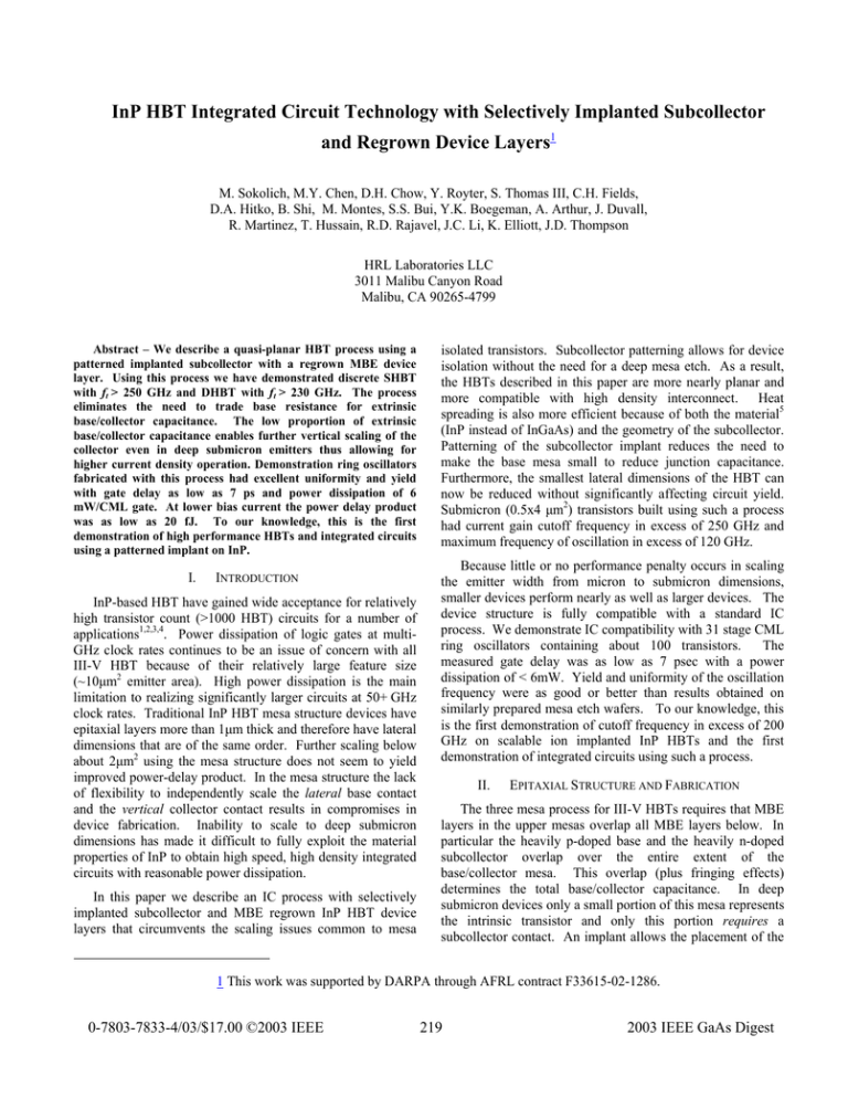
InP HBT Integrated Circuit Technology with Selectively Implanted Subcollector and Regrown Device Layers1 M. Sokolich, M.Y. Chen, D.H. Chow, Y. Royter, S. Thomas III, C.H. Fields, D.A. Hitko, B. Shi, M. Montes, S.S. Bui, Y.K. Boegeman, A. Arthur, J. Duvall, R. Martinez, T. Hussain, R.D. Rajavel, J.C. Li, K. Elliott, J.D. Thompson HRL Laboratories LLC 3011 Malibu Canyon Road Malibu, CA 90265-4799 Abstract – We describe a quasi-planar HBT process using a patterned implanted subcollector with a regrown MBE device layer. Using this process we have demonstrated discrete SHBT with ft > 250 GHz and DHBT with ft > 230 GHz. The process eliminates the need to trade base resistance for extrinsic base/collector capacitance. The low proportion of extrinsic base/collector capacitance enables further vertical scaling of the collector even in deep submicron emitters thus allowing for higher current density operation. Demonstration ring oscillators fabricated with this process had excellent uniformity and yield with gate delay as low as 7 ps and power dissipation of 6 mW/CML gate. At lower bias current the power delay product was as low as 20 fJ. To our knowledge, this is the first demonstration of high performance HBTs and integrated circuits using a patterned implant on InP. I. INTRODUCTION InP-based HBT have gained wide acceptance for relatively high transistor count (>1000 HBT) circuits for a number of applications1,2,3,4. Power dissipation of logic gates at multiGHz clock rates continues to be an issue of concern with all III-V HBT because of their relatively large feature size (~10µm2 emitter area). High power dissipation is the main limitation to realizing significantly larger circuits at 50+ GHz clock rates. Traditional InP HBT mesa structure devices have epitaxial layers more than 1µm thick and therefore have lateral dimensions that are of the same order. Further scaling below about 2µm2 using the mesa structure does not seem to yield improved power-delay product. In the mesa structure the lack of flexibility to independently scale the lateral base contact and the vertical collector contact results in compromises in device fabrication. Inability to scale to deep submicron dimensions has made it difficult to fully exploit the material properties of InP to obtain high speed, high density integrated circuits with reasonable power dissipation. In this paper we describe an IC process with selectively implanted subcollector and MBE regrown InP HBT device layers that circumvents the scaling issues common to mesa isolated transistors. Subcollector patterning allows for device isolation without the need for a deep mesa etch. As a result, the HBTs described in this paper are more nearly planar and more compatible with high density interconnect. Heat spreading is also more efficient because of both the material5 (InP instead of InGaAs) and the geometry of the subcollector. Patterning of the subcollector implant reduces the need to make the base mesa small to reduce junction capacitance. Furthermore, the smallest lateral dimensions of the HBT can now be reduced without significantly affecting circuit yield. Submicron (0.5x4 µm2) transistors built using such a process had current gain cutoff frequency in excess of 250 GHz and maximum frequency of oscillation in excess of 120 GHz. Because little or no performance penalty occurs in scaling the emitter width from micron to submicron dimensions, smaller devices perform nearly as well as larger devices. The device structure is fully compatible with a standard IC process. We demonstrate IC compatibility with 31 stage CML ring oscillators containing about 100 transistors. The measured gate delay was as low as 7 psec with a power dissipation of < 6mW. Yield and uniformity of the oscillation frequency were as good or better than results obtained on similarly prepared mesa etch wafers. To our knowledge, this is the first demonstration of cutoff frequency in excess of 200 GHz on scalable ion implanted InP HBTs and the first demonstration of integrated circuits using such a process. II. EPITAXIAL STRUCTURE AND FABRICATION The three mesa process for III-V HBTs requires that MBE layers in the upper mesas overlap all MBE layers below. In particular the heavily p-doped base and the heavily n-doped subcollector overlap over the entire extent of the base/collector mesa. This overlap (plus fringing effects) determines the total base/collector capacitance. In deep submicron devices only a small portion of this mesa represents the intrinsic transistor and only this portion requires a subcollector contact. An implant allows the placement of the 1 This work was supported by DARPA through AFRL contract F33615-02-1286. 0-7803-7833-4/03/$17.00 ©2003 IEEE 219 2003 IEEE GaAs Digest subcollector only where it is required as shown in Fig. 1. The planar process results in 2 distinct reductions of the overall device vertical dimension resulting in a quasi-planar transistor. The first reduction comes from the direct omission of the isolation mesa etch to remove the heavily doped subcollector between transistors. The second reduction comes from the scaling of the collector made possible by the reduction in extrinsic overlap area of the base and subcollector. In our device the mesa height was reduced from 1.1 µm to < 0.6 µm. InGaAs Base Layer description AlInAs Emitter InGaAs Collector N+ implant S.I. InP Subcollector Figure 1-Schematic cross section of device structure. To realize the patterned subcollector, Si was implanted at 80 keV (2.5x10¹⁴ /cm2) and 240 keV (5x10¹⁴ /cm2) into masked S.I. InP substrates. Mask openings as small as 0.25µm were used. The mask was then removed and the wafers annealed with a phosphine overpressure at 700C. A SIMS profile from a companion wafer is shown in Fig. 2. The AlInAs/InGaAs/(InGaAs or InP) epitaxial structures for this work were grown by gas source molecular beam epitaxy (GSMBE). All layers were grown lattice matched on semiinsulating InP substrates and the p-type and n-type dopants were beryllium and silicon, respectively. The basic SHBT structure has been reported previously8. The MBE growth omitted the subcollector (now realized by implantation) and reduced the collector thickness to 100 nm. The MBE profile of the DHBT device is shown in Fig. 3. FILE: H1180t01 2 Jun 2003 Cs CONCENTRATION (atoms/cc) 1E+20 S815-42 1E+19 1E+18 1E+17 1E+16 0 0.5 1 DEPTH (microns) Thickness (Å) Doping Level (cm-3) MBE InGaAs contact 1100 n:2.1E19 MBE InAlAs emitter contact 400 n:1.0E19 MBE InAlAs emitter 1050 n:1.3E18 MBE Chirped SLs 231 n:1.3E18 MBE InGaAs base layer 325 p:2.9E19 MBE Quaternary grade InP Collector 980 n:1.0E17 Figure 3-Schematic DHBT MBE layer structure (Implanted subcollector not shown). Emitters with measured dimensions as small as 0.35 µm were patterned on the wafer. The base dimensions could be made arbitrarily large without much impact to the base/collector capacitance but 0.5 µm was considered sufficient to minimize base contact resistance. Measured base contact resistivity (from TLM patterns) was 2x10⁻⁷ Ωcm2. The base sheet resistance was 650 Ω/□. Emitter access resistance was 20 Ω µm2 including both contact and bulk semiconductor resistance of the emitter cap. The subcollector sheet resistance was about 22 Ω/□. Other details of the process have been reported previously6. The interlayer dielectric was planarized in an Inductively Coupled Plasma (ICP) etcher which is also used to define the via contacts7. The mask used to pattern devices on this lot was not fully optimized for the implantation and so did not contain the minimum base/collector overlap possible. However, the results in the next section indicate that the process is IC compatible and preserves yield and uniformity of HBTs. III. DEVICE PERFORMANCE A forward Early characteristic of a 0.5x4 µm2 SHBT transistor is shown in figure 4. Current gain for this device was well over 150 indicating a very high quality base-layer growth on the implanted substrate. Maximum current density in the devices was about 700 kA/cm2. Breakdown (BVceo) on the SHBT transistors with 100nm collector was 3.1V. A similar characteristic is shown in figure 5 for a DHBT grown on a wafer from the same implant lot. The current gain is somewhat lower but the breakdown is much higher at about 4.5V. The maximum current gain for the DHBT was greater than 70. These high values of current gain indicate that the base layer was of extremely high quality even though significant wafer processing occurred before the MBE growth. We obtained 250 GHz ft on SHBTs and 230 GHz ft on DHBTs (Vce = 1V, Ic = 10 mA). Fig. 6 shows the extrapolated ft from de-embedded s-parameter measurements to 110 GHz. Fig. 7 shows the ft dependence on device current (approximate emitter area = 2 µm2). The ft extrapolations in Figure 7 are from single frequency measurement at 40 GHz at each current bias. The collector emitter potential (Vce) for the measurements in Fig. 7 was 1.5V. Figure 2- SIMS depth profile of Si implanted subcollector. 220 300 15 SHBT Cutoff Frequency (GHz) Collector Current, mA s815_039_MS_p54_ ∆ib = 14 µ A 10 5 0 0 0.5 1 1.5 Collector Current, mA 1.00 10.00 100.00 CIRCUIT PERFORMANCE A number of 15 and 31-stage ring oscillators were tested with device sizes ranging from 0.35x1 µm2 to 1x3 µm2. Load resistors in the CML gates were realized by ion implantation. Figure 8 is a photomicrograph of one of the 31-stage ring oscillator circuits (utilizing 0.5x4 µm2 HBT described previously). Gate delay and power dissipation for a range of bias currents (externally applied) is shown in figure 9. Note that the logic swing changes but is > 250 mV for bias current above 2.5 mA/stage. 5 0 1 1.5 2 Collector-Emitter Potential, V Figure 5-Forward Early characteristic of 0.5x4µm2 InP DHBT with implanted subcollector. Vce = 1V Because our new process requires substantial modification to the growth of the device epitaxial material, one of our priorities was to investigate the uniformity and yield of transistors. The ring oscillators provide a simple method to evaluate both. Figure 10 shows the distribution of calculated CML gate delay of 31-stage ring oscillators on the SHBT wafer. The yield of these 100 transistor circuits was excellent with significant clustering so that there was no yield loss attributable to HBTs in the center 80% of the wafer. The yield results give further indication that the MBE epitaxial layers were of very high quality. Given these yield and uniformity results we would expect demonstration circuits with 1000 transistors to be possible. SHBT h 21 DHBT 10 250 GHz 230 GHz 1 10 50 A key motivation to use implanted subcollector HBTs instead of further scaled mesa HBTs is to achieve performance gains without sacrificing IC producibility or yield. In this section we review early circuit results from demonstration vehicles using a 2-level metal process. 10 1 100 IV. ∆ib = 44 µ A 100 150 Figure 7-Unity current gain cutoff frequency (ft) of 0.5x4 µm2 InP SHBT and DHBT with implanted subcollector. s815_041_s0.54_M 0.5 200 Collector Current (mA) Figure 4-Forward Early characteristic of 0.5x4µm2 InP SHBT with implanted subcollector. 0 DHBT 0 0.10 2 Collector-Emitter Potential, V 15 250 100 1000 Frequency (GHz) Figure 6-De-embedded h21 as a function of frequency for both SHBT and DHBT devices with implanted subcollector. 221 subcollector implant. In this case power delay product is a better comparison of the circuit performance. Power delay product was as low as 20 fJ which is comparable to the mesa HBT process with the same device geometry. V. Figure 8-31-stage ring oscillator circuit employing the 0.5x4µm SHBT and CML inverters. The circuit contains about 100 SHBTs. 20 Gate Delay, psec 15 ∆ V = 63 mV 10 10 ∆ V = 250 mV 5 0 0 50 Power per Gate, mW 100 Current 8 7 6 Count 5 4 3 2 1 5 6 7 VI. 8 9 10 Propagation Delay (psec) Figure 10-Distribution of CML gate delay on one wafer. The yield and uniformity results are comparable to our mesa HBT processes. The gate delay is greater than we had previously reported8 on mesa HBT with similar structures mainly due to non-optimum load resistances defined by the ACKNOWLEDGEMENT This work was supported by DARPA through AFRL contract F33615-02-1286. We thank John Zolper of DARPA, and John King and Mark Pacer of AFRL for their support. We also thank Dr. Bill Stanchina, director of the HRL Microelectronics Laboratory, for his encouragement. VII. 1 Figure 9-Gate delay and power dissipation per gate extracted from 31-stage ring oscillator as a function of total circuit current. Vee = -3.0 V. 0 We have demonstrated an integrated circuit process utilizing a patterned ion implantation step to define the HBT subcollector. High quality MBE material comparable to that grown on virgin InP substrates has been grown on the annealed surface. Using this process we have demonstrated devices with unity current gain cutoff frequency (ft) as high as 250 GHz. We have also demonstrated highly uniform device characteristics and yield at the 100 HBT level with ring oscillators. The ring oscillators had gate delay as low as 7 psec and power delay product as low as 20 fJ. Through further optimization of the base/subcollector overlap, this technology has the potential of producing high yield, high performance HBTs with deep submicron dimensions. 1 150 100 SUMMARY REFERENCES G. Georgiou. Y. Baeyens. Y.-K. Chen, A. H. Gnauck, C. Gröpper, P. Paschke, R. Pullela, M. Reinhold, C. Dorschky, J.-P. Mattia, T. W. von Mohrenfels, and C. Schulien “Clock and Data Recovery IC for 40-Gb/s FiberOptic Receiver” JSSC, Vol 37, No. 9, Sep 2002, pp. 1120-1125. 2 K. Ishii, H. Nakajima, H. Nosaka, M. Ida, K. Kurishima, S. Yamahata, T. Enoki and T. Shibata, “Over 40 Gb/s 16:1 Multiplexer IC Using Inp/InGaAs HBT Technology” Electronics Lett. Vol. 39, No. 12, June 2003, pp. 911-913. 3 A. Hendarman, E.A. Sovero, X. Xu, K. Witt, “STS-768 Multiplexer with Full Rate Output Data Retimer in InP HBT” 2002 IEEE GaAs IC Symp. Tech Dig., pp. 211-215. 4 A. Gutierrez-Aitken, J. Matsui, E.N. Kaneshiro, B.K. Oyama, D. Sawdai, A.K. Oki, D.C. Streit, “Ultrahigh-Speed Direct Digital Synthesizer Using InP DHBT Technology”, IEEE Journal of Solid State Circuits, Vol 37, No. 9, Sept. 2002, pp. 1115-1121. 5 H. Masuda, K. Ouchi, A. Terano, H. Suzuki, K. Watanabe, T. Oka, H. Matsubara, and T. Tanoue, “Device Technology of InP/InGaAs HBTs for 40Gb/s Optical Transmission Application”, 1997 GaAs IC Symposium Digest. 6 S. Thomas, “Fabrication of InP-based Integrated Circuits”, Indium Phosphide and Related Materials Conference Proceedings, 2000. 7 S. Thomas, C.H. Fields, J.J. Brown, M. Sokolich, R. Martinez, and B. Doty, “Dry Etching of Polyimide Vias Using an Inductively Coupled Plasma Source: Model and Experiment”, 1998 GaAs ManTech, pp. 27-30. 8 M. Sokolich, A.R. Kramer, Y.K. Boegeman, R.R. Martinez, “Demonstration of sub-5 ps CML ring oscillator gate delay with reduced parasitic AlInAs/InGaAs HBT”, IEEE Electron Device Lett., Vol. EDL-22, pp. 309311, July 2001. 222


