AFBR-15x9Z
DC to 10 Mbd Versatile Link Fiber Optic
Analog Transmitter for 1 mm POF and 200 µm PCS
Data Sheet
Description
Features
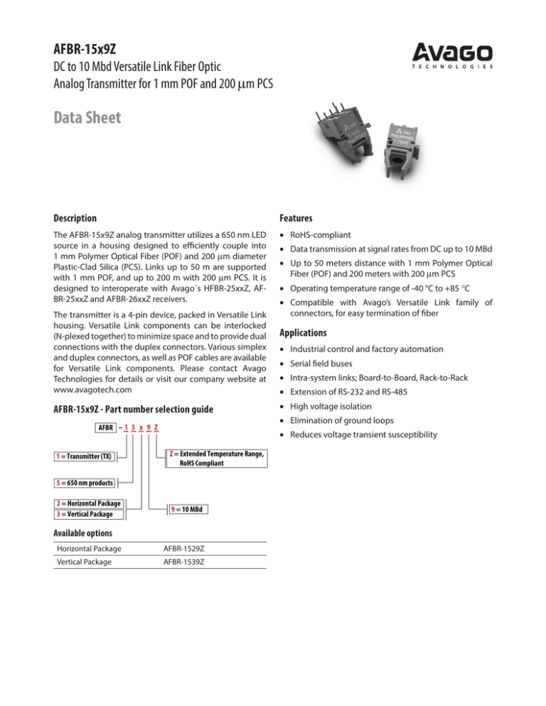
The AFBR-15x9Z analog transmitter utilizes a 650 nm LED
source in a housing designed to efficiently couple into
1 mm Polymer Optical Fiber (POF) and 200 µm diameter
Plastic-Clad Silica (PCS). Links up to 50 m are supported
with 1 mm POF, and up to 200 m with 200 µm PCS. It is
designed to interoperate with Avago´s HFBR-25xxZ, AFBR-25xxZ and AFBR-26xxZ receivers.
• RoHS-compliant
The transmitter is a 4-pin device, packed in Versatile Link
housing. Versatile Link components can be interlocked
(N-plexed together) to minimize space and to provide dual
connections with the duplex connectors. Various simplex
and duplex connectors, as well as POF cables are available
for Versatile Link components. Please contact Avago
Technologies for details or visit our company website at
www.avagotech.com
AFBR-15x9Z - Part number selection guide
AFBR – 1 5 x 9 Z
1 = Transmitter (TX)
• Up to 50 meters distance with 1 mm Polymer Optical
Fiber (POF) and 200 meters with 200 µm PCS
• Operating temperature range of -40 °C to +85 °C
• Compatible with Avago’s Versatile Link family of
connectors, for easy termination of fiber
Applications
• Industrial control and factory automation
• Serial field buses
• Intra-system links; Board-to-Board, Rack-to-Rack
• Extension of RS-232 and RS-485
• High voltage isolation
• Elimination of ground loops
• Reduces voltage transient susceptibility
Z = Extended Temperature Range,
RoHS Compliant
5 = 650 nm products
2 = Horizontal Package
3 = Vertical Package
• Data transmission at signal rates from DC up to 10 MBd
9 = 10 MBd
Available options
Horizontal Package
AFBR-1529Z
Vertical Package
AFBR-1539Z
Package and Handling Information
Handling
Versatile Link packages are made of a flame-retardant
material and use the same pad layout as a standard,
eight-pin dual-in-line package. Versatile Link packages
are stackable and are enclosed to provide a dust-resistant
seal. Snap action simplex, simplex latching, duplex, and
duplex latching connectors are offered with simplex or
duplex cables.
Versatile Link components are auto-insertable. When wave
soldering is performed with Versatile Link components,
the optical port plug should be left in to prevent contamination of the port. Do not use reflow solder processes (i.e.,
infrared reflow or vapor-phase reflow). Non-halogenated
water-soluble fluxes (i.e., 0% chloride), not rosin-based
fluxes, are recommended for use with Versatile Link components.
Package Housing Color
Versatile Link components and simplex connectors are
color-coded to eliminate confusion when making connections. Transmitters are gray.
Versatile Link components are moisture-sensitive devices
and are shipped in a moisture-sealed bag. If the components are exposed to air for an extended period of time,
they may require a baking step before the soldering
process. Refer to the special labeling on the shipping tube
for details.
Mechanical Dimensions
Horizontal Module
Vertical Module
2.03
(0.080)
6.86
(0.270)
10.16
(0.400)
5.08
(0.200)
18.8
(0.74)
0.64
(0.025)
7.62
(0.30)
7.62
(0.300)
3.81 (0.150) MAX.
3.56 (0.140) MIN.
0.64 (0.025) DIA.
2.77
(0.109)
1.85
(0.073)
DIMENSIONS IN MILLIMETERS (INCHES)
2
4.19
(0.165)
0.51
(0.020)
1.27
(0.050)
2.54
(0.100)
2.03
(0.080)
5.08
10.16 (0.200)
(0.400)
6.86
(0.27)
18.80
(0.740)
18.29
(0.720)
Versatile Link Printed Board Layout Dimensions
Horizontal Module
7.62
(0.300)
2.54
(0.100)
TOP VIEW
Vertical Module
1.01 (0.040) DIA.
4 3 2 1
5
7.62
(0.300)
TOP VIEW
PCB EDGE
8
1.85 MIN.
(0.073)
DIMENSIONS IN MILLIMETERS (INCHES).
Interlocked (Stacked) Assemblies
Horizontal packages may be stacked by placing units
with pins facing upward. Initially engage the inter­
locking mechanism by sliding the L bracket body from
above into the L slot body of the lower package. Use
a straight edge, such as a ruler, to bring all stacked
units into uniform alignment. This tech­nique prevents
potential harm that could occur to fingers and hands of
assemblers from the package pins. Stacked horizontal
packages can be disengaged if necessary. Repeated
stacking and unstack­ing causes no damage to individual
units.
Stacking Horizontal Modules
Stacking Vertical Modules
3
To stack vertical packages, hold one unit in each hand,
with the pins facing away and the optical ports on the
bottom. Slide the L bracket unit into the L slot unit. The
straight edge used for horizontal package alignment is
not needed.
Pin Description Transmitter
VCC
R1
C1
R2
C2
AFBR-15x9Z
1
Fiber port facing front, pins downward, 1 = Rightmost pin to 4 = Leftmost pin
8
2
3
68
4
5
5
1/2 SN75451
DATA
7
4
Note:
This is an inverting circuitry, thus the
LED is off in case of DATA "H". Therefore,
an inverting receiver, e.g. AFBR-2529Z,
should be used accordingly.
Value Tolerance
R1
2 kΩ
5%
R2
100 Ω
1%
C1
0.1 μF
20%
C2
10 μF
20%
Pin
Name
Function/Description
Notes
1
Anode
LED Anode
2
Cathode
LED Cathode
3
Pin
No function, physical pin available,
recommended to signal GND
4
Pin
No function, physical pin available,
recommended to signal GND
5
Housing Pin Physical pin available,
recommended to chassis GND
1
8
Housing Pin Physical pin available,
recommended to chassis GND
1
Figure 1. Recommended drive circuit Top View
(IF,on = 30 mA nominal at TA = 25 °C)
Regulatory Compliance
Feature
Test Method
Performance
Electrostatic Discharge (ESD) to the Electrical Pins Human Body Model
MIL-STD-883 Method 3015
Min ± 2000 V
Eye Safety
IEC 60825-1,2 ,Class 1
Class 1
Specified Link Performance, TA = -40 °C to +85 °C, 10 MBd
Parameter
Min
Max
Unit
Condition
Note
Link Distance with Standard Loss POF cable
0.1
50
m
-40 °C to +85 °C
2
Link Distance with 200 µm PCS cable
0.1
200
m
-40 °C to +85 °C
3
Notes:
1. Pins 5 and 8 are for mounting and retaining purposes. Make sure they are electrically connected to Chassis GND.
2. POF is HFBR-R/EXXYYYZ plastic (1 mm) optical fiber. Worst-case attenuation used (0.27 dB/m for standard loss POF cable from -40 °C to +85 °C at
650 nm). Link performance is valid in combination with AFBR-26x4Z and AFBR-25x9Z.
3. PCS, worst-case attenuation (12 dB/km from -40 °C to +85 °C at 650 nm).
4
Absolute Maximum Ratings
Parameter
Symbol
Min
Max
Unit
Notes
Storage and Operating Temperature
TS,O
-40
85
°C
Transmitter Peaking Forward Input Current
IF,PK
45
mA
1
Transmitter Short Term Peaking Forward Input Current
IF, PKshort
80
mA
2
Transmitter Average Forward Input Current
IF,AVG
30
mA
Transmitter Reverse Input Voltage
VR
3
V
Notes:
1. For IF,PK > 30 mA the duty factor must maintain ≤ 30 mA IF,AVG and pulse width ≤ 1 ms
2. Maximum short term peaking forward current must not longer be applied than 5 ns to improve rise time or enhance signaling rate. Applying a
short term peaking forward current shall not result in exceeding 30 mA average forward current.
Recommended Operating Conditions
Parameter
Symbol
Min
Max
Unit
Notes
Ambient Temperature, no air flow
TA
-40
85
°C
1, 2
Transmitter Average Forward Input Current
IF,AVG
3
30
mA
Signaling Rate
fs
DC
10
Mbd
3
Notes:
1. Recommended operating conditions are those values outside of which functional performance is not intended, device reliability is not implied,
and damage to the device may occur over an extended period of time. See Reliability Data Sheet for specific reliability performance.
2. Measured at the housing.
3. Without peaking of the electrical input signal
Process Compatibility
Parameter
Symbol
Solder Environment
Max
Unit
Notes
TSOLD
260
°C
1, 3, 4
tSOLD
10
sec
2, 3, 4
Notes:
1. Maximum temperature refers to peak temperature.
2. Maximum time refers to time spent at peak temperature.
3. Solder surface to be at least 1 mm below lead frame stops.
4. Product is Moisture Sensitive Level 3.
5
Min
Typical
AFBR-15x9Z analog Transmitter
The AFBR-15x9Z analog transmitter utilizes a 650 nm LED source in a housing designed to efficiently couple into 1 mm
Polymer Optical Fiber (POF) or 200 µm Plastic-Clad Silica (PCS). Links up to 50 meters are supported with 1 mm POF.
Links up to 200 meters are supported with 200 µm PCS.
Electrical and Optical Characteristics
(TA = -40° C to +85° C unless otherwise stated)
Parameter
Symbol
Min
Typical
Max
Unit
Conditions
Notes
Peak Output Power, 1 mm POF, 30 mA
PT
-6
-1
2
dBm
IF,DC = 30 mA
1, 2
Peak Output Power, 200 µm PCS, 30 mA
PT
-18
-12
-9
dBm
IF,DC = 30 mA
1, 2
Peak Output Power, 1 mm POF, 10 mA
PT
-11
-6
-3
dBm
IF,DC = 10 mA
1, 2
Peak Output Power, 1 mm POF, 5 mA
PT
-14
-9
-6
dBm
IF,DC = 5 mA
1, 2
Peak Output Power, 1 mm POF, 3 mA
PT
-16
-11
-8
dBm
IF,DC = 3 mA
1, 2
Optical Power Temperature Coefficient
ΔPT/ΔT
-0.01
dB/K
-40 °C…+25 °C
Optical Power Temperature Coefficient
ΔPT/ΔT
-0.02
dB/K
+25 °C…+85 °C
Peak emission wavelength
λP
Peak Emission wavelength
Temperature coefficient
Δλ/ΔT
0.16
nm/K
Spectral Width
FWHM
20
nm
Forward Voltage
VF
Forward Voltage temperature coefficient
ΔVF/ΔT
Reverse Input Breakdown voltage
630
650
685
1.4
9
Diode Capacitance
2.3
nm
V
IF,DC = 3 mA to 30 mA
1.6
mV/K
IF,DC = 30 mA
20
V
30
70
pF
Optical Rise time
tr
30
ns
20% to 80%
3
Optical Fall time
tf
30
ns
80% to 20%
3
Notes:
1. Optical power measured with polished connector end face at the end of 0.5 meters of 1 mm diameter POF with a numerical aperture (NA) of 0.5,
or of 200 µm diameter PCS, with NA=0.37.
2. Minimum average output power specification value includes 1dB degradation margin.
3. Using recommended drive circuit in Figure 1 for IF,DC =30mA
2.3
2.1
0
PT - OUTPUT POWER - dBm
2.2
VF - FORWARD VOLTAGE - V
2
–40 °C
25 °C
85 °C
2
1.9
1.8
1.7
1.6
1.5
1.4
-2
-4
-6
-8
-10
–40 °C
25 °C
85 °C
-12
-14
1
10
IF - TRANSMITTER DRIVE CURRENT - mA
100
Figure 2. Typical forward voltage vs. drive current
For product information and a complete list of distributors, please go to our web site:
-16
1
10
IF - TRANSMITTER DRIVE CURRENT - mA
Figure 3. Typical optical output power vs. drive current
www.avagotech.com
Avago, Avago Technologies, and the A logo are trademarks of Avago Technologies in the United States and other countries.
Data subject to change. Copyright © 2005-2015 Avago Technologies. All rights reserved.
AV02-4367EN - April 13, 2015
100


