A 2-V 2.3/4.6-GHz Dual-Band Frequency Synthesizer in 0.35
advertisement
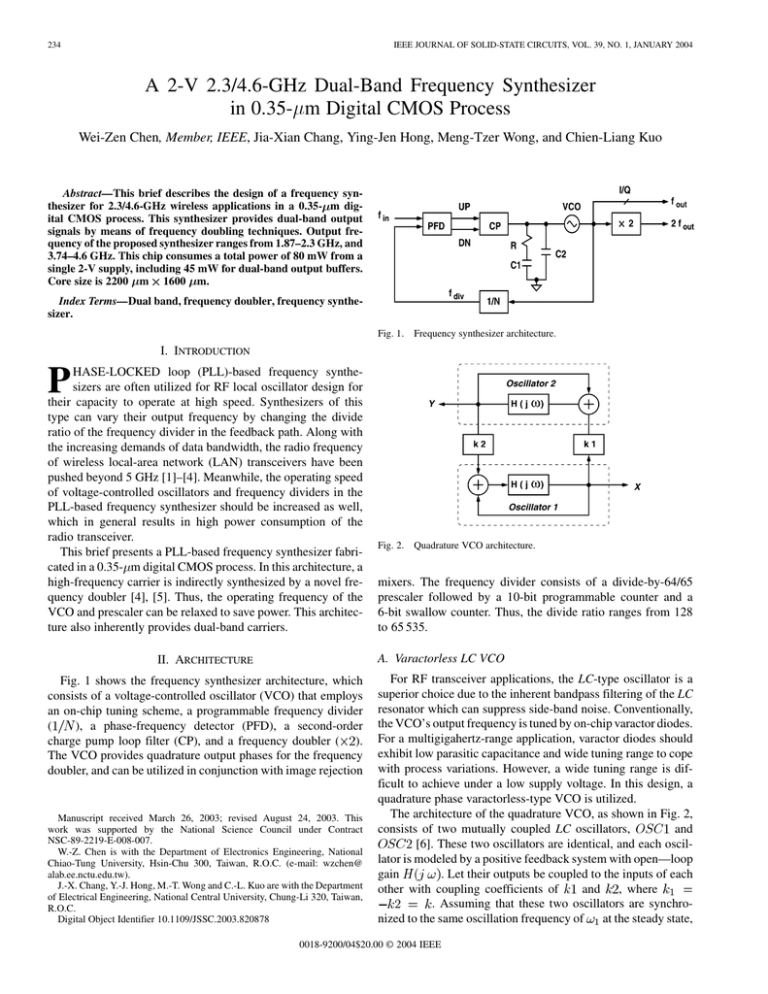
234 IEEE JOURNAL OF SOLID-STATE CIRCUITS, VOL. 39, NO. 1, JANUARY 2004 A 2-V 2.3/4.6-GHz Dual-Band Frequency Synthesizer in 0.35-m Digital CMOS Process Wei-Zen Chen, Member, IEEE, Jia-Xian Chang, Ying-Jen Hong, Meng-Tzer Wong, and Chien-Liang Kuo Abstract—This brief describes the design of a frequency synthesizer for 2.3/4.6-GHz wireless applications in a 0.35- m digital CMOS process. This synthesizer provides dual-band output signals by means of frequency doubling techniques. Output frequency of the proposed synthesizer ranges from 1.87–2.3 GHz, and 3.74–4.6 GHz. This chip consumes a total power of 80 mW from a single 2-V supply, including 45 mW for dual-band output buffers. Core size is 2200 m 1600 m. Index Terms—Dual band, frequency doubler, frequency synthesizer. Fig. 1. Frequency synthesizer architecture. I. INTRODUCTION P HASE-LOCKED loop (PLL)-based frequency synthesizers are often utilized for RF local oscillator design for their capacity to operate at high speed. Synthesizers of this type can vary their output frequency by changing the divide ratio of the frequency divider in the feedback path. Along with the increasing demands of data bandwidth, the radio frequency of wireless local-area network (LAN) transceivers have been pushed beyond 5 GHz [1]–[4]. Meanwhile, the operating speed of voltage-controlled oscillators and frequency dividers in the PLL-based frequency synthesizer should be increased as well, which in general results in high power consumption of the radio transceiver. This brief presents a PLL-based frequency synthesizer fabricated in a 0.35- m digital CMOS process. In this architecture, a high-frequency carrier is indirectly synthesized by a novel frequency doubler [4], [5]. Thus, the operating frequency of the VCO and prescaler can be relaxed to save power. This architecture also inherently provides dual-band carriers. Fig. 2. Quadrature VCO architecture. mixers. The frequency divider consists of a divide-by-64/65 prescaler followed by a 10-bit programmable counter and a 6-bit swallow counter. Thus, the divide ratio ranges from 128 to 65 535. A. Varactorless LC VCO II. ARCHITECTURE Fig. 1 shows the frequency synthesizer architecture, which consists of a voltage-controlled oscillator (VCO) that employs an on-chip tuning scheme, a programmable frequency divider ), a phase-frequency detector (PFD), a second-order ( charge pump loop filter (CP), and a frequency doubler ( ). The VCO provides quadrature output phases for the frequency doubler, and can be utilized in conjunction with image rejection Manuscript received March 26, 2003; revised August 24, 2003. This work was supported by the National Science Council under Contract NSC-89-2219-E-008-007. W.-Z. Chen is with the Department of Electronics Engineering, National Chiao-Tung University, Hsin-Chu 300, Taiwan, R.O.C. (e-mail: wzchen@ alab.ee.nctu.edu.tw). J.-X. Chang, Y.-J. Hong, M.-T. Wong and C.-L. Kuo are with the Department of Electrical Engineering, National Central University, Chung-Li 320, Taiwan, R.O.C. Digital Object Identifier 10.1109/JSSC.2003.820878 For RF transceiver applications, the LC-type oscillator is a superior choice due to the inherent bandpass filtering of the LC resonator which can suppress side-band noise. Conventionally, the VCO’s output frequency is tuned by on-chip varactor diodes. For a multigigahertz-range application, varactor diodes should exhibit low parasitic capacitance and wide tuning range to cope with process variations. However, a wide tuning range is difficult to achieve under a low supply voltage. In this design, a quadrature phase varactorless-type VCO is utilized. The architecture of the quadrature VCO, as shown in Fig. 2, and consists of two mutually coupled LC oscillators, [6]. These two oscillators are identical, and each oscillator is modeled by a positive feedback system with open—loop . Let their outputs be coupled to the inputs of each gain and , where other with coupling coefficients of . Assuming that these two oscillators are synchroat the steady state, nized to the same oscillation frequency of 0018-9200/04$20.00 © 2004 IEEE IEEE JOURNAL OF SOLID-STATE CIRCUITS, VOL. 39, NO. 1, JANUARY 2004 235 Fig. 3. VFO circuit schematic. the output phasors ) must satisfy of the two oscillators ( and Fig. 4. Frequency doubler. (1) (2) The combination of these two equations indicates that Thus, quadrature phases can be derived at the VCO outputs. The oscillation frequency can be determined by substituting into (1) or (2), which yields the frequency tuning characteristic equations, as follows: (3) (4) There will be two solutions, and , which correspond to positive and negative sign, that both satisfy (4). However, only that is closer to the resonant frethe oscillation frequency ’s phase requency of the LC-tank can be sustained. As sponse can be varied by adjusting the coupling coefficient , the VCO’s output frequency can be changed accordingly [6]. The detailed circuit schematic of the quadrature phase VCO is composed of (M1, M2, M9, is shown in Fig. 3. Here, L1, L2), and is composed of (M5, M6, M12, L3, L4). These two oscillators are mutually coupled by two differential amplifiers (M3, M4, M10) and (M7, M8, M11), and the coupling coefficient is determined by the current source M14. The VCO’s output frequency can be varied by tuning the bias voltage . In order to avoid loss of coupling in the extreme case of frequency tuning, i.e., approaching zero, an extra current source is added in parallel to M14. Thus, quadrature output phases can be maintained at any output frequency. be represented Let the VCO’s outputs at , , , and , , , and as . The drain voltages of M10 and M11 can be derived as and will be Equations (5) and (6) show that modulated by the second-order harmonic of the VCO’s oscillation frequency, which will result in tail current variation due to the finite output resistance of the current source. As long as is out of phase to that of the tail current variation of , in the steady state, the summation of the and switching currents should approximate a constant. In together with are biased at a conthis design, stant current source M13. Thus, the tail current variation can be alleviated. From another viewpoint, the constant current biased scheme becomes another constraint to synchronize quadrature phases at VCO output and improves amplitude matching. Also, the proposed architecture could improve phase noise performance by suppressing AM-to-PM noise conversion. B. Frequency Doubler The proposed frequency doubler is depicted in Fig. 4. By means of phase mixing, the pulsewidth of the differential amplifier is reduced to 1/4 VCO period, which results in double frequency at the output. The NAND functions of the quadrature phases are decomposed into four pass transistor logic in parallel and swap-connected to balance the loading effects as seen by the VCO. Moreover, inductive loads are employed in the frequency doubler to speed up voltage switching. On the other hand, the inductive loads perform as a resonator in conjunction with parasitic capacitance at the output node. This provides bandpass filtering to suppress spurious tones caused by phase mixing. According to simulation results, the output power variation of the frequency doubler is less than 0.5 dB while the spurious free dynamic range is higher than 50 dB with phase mismatches larger than 5%. This indicates that the frequency doubler has high immunity to phase mismatch due to its fully symmetrical architecture and bandpass filtering. In this prototype, (L1, L2) of the frequency doubler are made up of bonding wires, and therefore, no extra on-chip spiral inductors are required. (5) III. EXPERIMENTAL RESULTS (6) Fig. 5 shows the measured VCO frequency transfer characteristic. The output frequency of the VCO ranges from 1.87 to IEEE JOURNAL OF SOLID-STATE CIRCUITS, VOL. 39, NO. 1, JANUARY 2004 2.5 5 VCO 2 4 Frequency Doubler 1.5 3 0.6 0.7 0.8 0.9 1 Output Frequency (GHz) Output Frequency (GHz) 236 1.1 1.2 1.3 1.4 1.5 1.6 Control Voltage (V) Fig. 5. Measured VCO frequency tuning characteristic. Fig. 7. Measured frequency doubler output spectrum. (a) Fig. 6. Measured VCO output spectrum. 2.3 GHz and from 3.74 to 4.6 GHz. The highest output frequency is limited by the prescaler. The conversion gain of the VCO is about 430 MHz/V. The loop bandwith is about 120 kHz and the damping factor is 0.55. The measured output spectrum at 2.33 GHz is shown in Fig. 6, while the frequency doubler output signal at 4.66 GHz is shown in Fig. 7. The measured phase noise plots of the 2.33 and 4.66 GHz carriers are shown in Fig. 8. At 5-MHz offset, the phase noise is 114 dBc/Hz and 100 dBc/Hz, respectively, from a 2.33- and 4.66-GHz output signal. The phase noise performance is improved by 3 dB at 2 GHz and 4 GHz as the output frequency is tuned to the resonant frequency of the LC tank. The measured frequency spurs are 60 and 48 dB below the main carrier at 2.3- and 4.6-GHz output, respectively. The reasons for moderate phase noise performance are mainly due to two factors. First, in this prototype, the conversion gain of the VCO is relatively high, which makes the VCO susceptible to noise coupling. Second, as the frequency of oscillation deviates from the resonance frequency of the of the tank is reduced. standalone oscillator, the effective This results in the degradation of phase noise performance. (b) Fig. 8. Phase noise plot at (a) 2.33 GHz and (b) 4.66 GHz. Fig. 9 shows the chip photograph of the frequency synthesizer, including a quadrature VCO, an on-chip loop filter, a frequency doubler, a programmable divider, and dual-band output buffers. Implemented in a 0.35- m digital CMOS process, the core area of the PLL occupies a chip area of IEEE JOURNAL OF SOLID-STATE CIRCUITS, VOL. 39, NO. 1, JANUARY 2004 237 are biased by a constant current source to improve both amplitude and phase matching performance. In addition, output phase noise is reduced by this constant current biased scheme. Finally, a novel frequency doubler is proposed in this design, which relaxes the operating speed of the VCO and prescaler. Thus, lower power consumption can be obtained. Doubled frequency output is indirectly synthesized by quadrature phase mixing. The inherent bandpass filtering of the frequency doubler can suppress the spurious tones caused by phase mixing. ACKNOWLEDGMENT Fig. 9. Die micrograph of the frequency synthesizer. 2200 m 1600 m. This chip is pad-limited by numerous modulus-control inputs. Under a single 2-V supply, this chip drains a total power of 80 mW, including 8 mW for the VCO core, and 45 mW for output buffers at both 2.3 and 4.6 GHz to drive 50- load. IV. CONCLUSION This paper describes the design of a single-chip dual-band frequency synthesizer in a low-cost digital CMOS process. In this design, a varactorless VCO composed of two identical oscillators is utilized. Frequency tuning is achieved by varying mutual coupling of the two fixed frequency oscillators. Quadrature output phases can be derived from the VCO. The two VCOs The authors would like to thank the National Science Council’s Chip Implementation Center for chip fabrication. REFERENCES [1] T. H. Lee and S. S. Wong, “CMOS RF integrated circuits at 5 GHz and beyond,” Proc. IEEE, vol. 88, pp. 1560–1571, Oct. 2000. [2] H. Samavati, H. R. Rategh, and T. H. Lee, “A 5-GHz CMOS wireless LAN receiver front end,” IEEE J. Solid-State Circuits, vol. 35, pp. 765–772, May 2000. [3] T. H. Lee, H. Samavati, and H. R. Rategh, “5-GHz CMOS wireless LANs,” IEEE Trans. Microwave Theory Tech., vol. 50, pp. 268–280, Jan. 2002. [4] C. Lam and B. Razavi, “A 2.6-GHz/5.2-GHz frequency synthesizer in 0.4-m CMOS technology,” IEEE J. Solid-State Circuits, vol. 35, pp. 788–794, May 2000. [5] W.-Z. Chen, J.-X. Chang, Y.-J. Hong, M.-T. Wong, and C.-L. Kuo, “A 2-V 2.3/4.6-GHz dual-band CMOS frequency synthesizer,” in IEEE RF IC Symp. Dig., June 2002, pp. 169–172. [6] T.-P. Liu, “A 6.5-GHz monolithic CMOS voltage-controlled oscillator,” in IEEE Int. Solid-State Circuits Conf. Dig. Tech. Papers, 1999, pp. 404–405.
