HMPP-386x Series
MiniPak Surface Mount RF PIN Diodes
Data Sheet
Description/Applications
Features
These ultra-miniature products represent the blending of
Avago Technologies’ proven semiconductor and the latest
in leadless packaging technology.
• Surface mount MiniPak package
The HMPP-386x series of general purpose PIN diodes are
designed for two classes of applications. The first is attenuators where current consumption is the most important
design consideration. The second application for this
series of diodes is in switches where low capacitance with
no reverse bias is the driving issue for the designer.
• Single and dual versions
The low dielectric relaxation frequency of the HMPP-386x
insures that low capacitance can be reached at zero volts
reverse bias at frequencies above 1 GHz, making this PIN
diode ideal for hand held applications.
Low junction capacitance of the PIN diode chip, combined
with ultra low package parasitics, mean that these products
may be used at frequencies which are higher than the upper
limit for conventional PIN diodes.
Note that Avago’s manufacturing techniques assure that
dice packaged in pairs are taken from adjacent sites on
the wafer, assuring the highest degree of match.
Minipak 1412 is a ceramic based package, while Minipak
QFN is a leadframe based package.
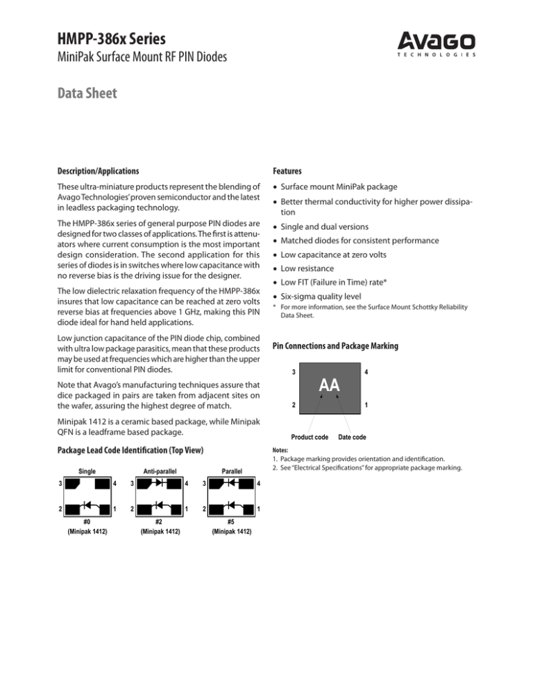
Package Lead Code Identification (Top View)
Single
3
2
#0
(Minipak 1412)
Anti-parallel
4
3
1
2
#2
(Minipak 1412)
3
1
2
4
1
#5
(Minipak 1412)
• Matched diodes for consistent performance
• Low capacitance at zero volts
• Low resistance
• Low FIT (Failure in Time) rate*
• Six-sigma quality level
* For more information, see the Surface Mount Schottky Reliability
Data Sheet.
Pin Connections and Package Marking
3
AA
2
Product code
4
1
Date code
Notes:
1. Package marking provides orientation and identification.
2. See “Electrical Specifications” for appropriate package marking.
Parallel
4
• Better thermal conductivity for higher power dissipation
HMPP-386x Series Absolute Maximum Ratings [1], Tc = 25°C
Symbol
Parameter
Units
MiniPak 1412 / MiniPak QFN
If
Forward Current (1 µs pulse)
Amp
1
PIV
Peak Inverse Voltage
V
100
Notes:
1. Operation in excess of any one of these
conditions may result in permanent damage to the device.
2. TC = +25°C, where TC is defined to be the
temperature at the package pins where
contact is made to the circuit board.
Tj
Junction Temperature
°C
150
ESD WARNING:
Tstg
Storage Temperature
°C
-65 to +150
Handling Precautions Should Be Taken
To Avoid Static Discharge.
θ jc Thermal Resistance [2]
°C/W
150
MiniPak1412
Electrical Specifications, Tc = +25°C, each diode
Part Number
HMPP-
Package
Marking Code
Lead Code
Configuration
Minimum Breakdown
Voltage (V)
Typical Series
Resistance (Ω)
3860
3862
3865
H
F
E
50
3.0/1.5*
VR = VBR
Measure
IR ≤ 10 µA
IF = 10 mA
f = 100 MHz
*IF = 100 mA
0
2
5
Single
Anti-parallel
Parallel
Test Conditions
MiniPak1412
Typical Parameters, Tc = +25°C
Part Number
HMPP-
Total Resistance
RT (Ω)
Carrier Lifetime
τ (ns)
Reverse Recovery Time
Trr (ns)
Total Capacitance
CT (pF)
3860
3862
3865
22
500
80
0.20
VR = 10 V
IF = 20 mA
90% Recovery
VR = 50V
f = 1 MHz
Test Conditions
IF = 1 mA
IF = 50 mA
f = 100 MHz
TR = 250 mA
MiniPak 1412 HMPP-386x Series Typical Performance
TC = +25 °C (unless otherwise noted), each diode
1000
1 MHz
0.25
100 MHz
0.20
0.15
1 GHz
0
2
4
6
8
100
10
1
0.01
10 12 14 16 18 20
0.1
Figure 1. RF Capacitance vs. Reverse Bias.
100
VR = 5 V
VR = 10 V
100
VR = 20 V
10
20
30
FORWARD CURRENT (mA)
Figure 4. Reverse Recovery Time vs. Forward
Current for Various Reverse Voltages.
10
1
0.1
0.01
125 C
0
0.2
0.4
25 C
0.6
–50 C
0.8
115
110
Diode Mounted as a
Series Switch in a
50 Microstrip and
Tested at 123 MHz
Intercept point
will be higher
at higher
frequencies
105
100
95
90
85
1
10
30
IF – FORWARD BIAS CURRENT (mA)
100
IF – FORWARD CURRENT (mA)
Trr – REVERSE RECOVERY TIME (ns)
10
Figure 2. Typical RF Resistance vs. Forward Bias
Current.
1000
1
BIAS CURRENT (mA)
REVERSE VOLTAGE (V)
10
120
TA = +85 C
TA = +25 C
TA = –55 C
INPUT INTERCEPT POINT (dBm)
0.30
RF RESISTANCE (OHMS)
TOTAL CAPACITANCE (pF)
0.35
1.0
VF – FORWARD VOLTAGE (mA)
Figure 5. Forward Current vs. Forward
Voltage.
1.2
Figure 3. 2nd Harmonic Input Intercept Point
vs. Forward Bias Current for Switch Diodes.
Typical Applications
RF COMMON
RF COMMON
2
3
1
4
RF 1
RF 2
BIAS 1
3
4
3
4
2
1
2
1
RF 1
RF 2
BIAS 2
BIAS
Figure 7. High Isolation SPDT Switch Using Dual Bias.
Figure 6. Simple SPDT Switch Using Only Positive Bias.
RF COMMON
VARIABLE BIAS
1
4
RF 1
3
4
2
1
3
2
3
4
2
1
3
4
1
2
2
1
4
3
RF IN/OUT
INPUT
RF 2
FIXED
BIAS
VOLTAGE
BIAS
Figure 9. Four Diode p Attenuator. See AN1048 for details.
Figure 8. Very High Isolation SPDT Switch, Dual Bias.
Figure 9. Four Diode π Attenuator. See AN1048 for details.
BIAS
3
4
3
4
2
1
2
1
Figure 10. High Isolation SPST Switch (Repeat Cells as Required).
Diode Lifetime and Resistance
Dielectric Relaxation Frequency and Diode Capacitance
The resistance of a PIN diode is controlled by the conductivity (or resistivity) of the I layer. This conductivity is
controlled by the density of the cloud of carriers (charges)
in the I layer (which is, in turn, controlled by the DC bias).
Minority carrier lifetime, indicated by the Greek symbol
τ, is a measure of the time it takes for the charge stored
in the I layer to decay, when forward bias is replaced with
reverse bias, to some predetermined value. This lifetime
can be short (35 to 200 nsec. for epitaxial diodes) or it
can be relatively long (400 to 3000 nsec. for bulk ­diodes).
Lifetime has a strong influence over a ­ number of PIN
diode parameters, among which are distortion and basic
diode behavior.
fDR (Dielectric Relaxation ­ Frequency) for a PIN ­ diode is
given by the equation
f = 1
To study the effect of lifetime on diode behavior, we first
define a cutoff frequency fC = 1/τ. For short lifetime diodes,
this cutoff frequency can be as high as 30 MHz while for
our longer lifetime diodes fC ≅ 400 KHz. At frequencies
which are ten times fC (or more), a PIN diode does indeed
act like a current controlled variable resistor. At frequencies which are one tenth (or less) of fC, a PIN diode acts
like an ordinary PN junction diode. Finally, at 0.1fC ≤ f ≤
10fC, the behavior of the diode is very complex. Suffice it
to mention that in this frequency range, the diode can
exhibit very strong capacitive or inductive reactance — it
will not behave at all like a resistor.
The HMPP-386x family features a typical lifetime of 300 to
500 ns, so 10fC for this part is 5 MHz. At any frequency over
5 MHz, the resistance of this diode will follow the curve
given in Figure 2. From this curve, it can be seen that the
HMPP-386x family produces a lower resistance at a given
value of bias current than most attenuator PIN diodes,
making it ideal for applications where current consumption is important.
DR
2πρε
where…
ρ = bulk resistivity of the I-layer
ε = ε0 εR = 10 -12 F/cm
= bulk susceptance of silicon
In the case of an epitaxial diode with a value for ρ of 10Ωcm, fDR will be in Ku-Band. For a bulk diode fabricated on
very pure material, ρ can be as high as 2000, resulting in
a value of fDR of 80 MHz.
The implications of a low fDR are very important in RF attenuator and switch circuits. At operating ­frequencies below
fDR, reverse bias (as much as 50V) is needed to minimize
junction capacitance. At operating frequencies well above
fDR, the curve of capacitance vs. reverse bias is flat.
For the HMPP-386x family, fDR is around 500 MHz, resulting
in very low capacitance at zero bias for frequencies above
1 GHz. See Figure 1.
Linear Equivalent Circuit
In order to predict the performance of the HMPP-386x
as a switch or an attenuator, it is necessary to ­construct a
model which can then be used in one of the several linear
analysis programs presently on the market. Such a model
is given in Figure 16, where RS + Rj is given in Figure 2 and
Cj is provided in Figure 1. Careful examination of Figure 16
will reveal the fact that the package parasitics (inductance
and capacitance) are much lower for the MiniPak than they
are for leaded plastic packages such as the SOT-23, SOT323 or ­others. This will permit the HMPP-386x family to be
used at higher frequencies than its conventional leaded
counterparts.
20 fF
3
30 fF
4
1.1 nH
2
30 fF
1
20 fF
Single diode package (HMPP-3860)
20 fF
3
2
0.05 nH
30 fF
0.05 nH
0.5 nH
0.5 nH
0.5 nH
0.05 nH
12 fF
30 fF
0.05 nH
0.5 nH
4
1
20 fF
Anti-parallel diode package (HMPP-3862)
20 fF
3
2
0.05 nH
30 fF
0.05 nH
0.5 nH
0.5 nH
0.5 nH
0.05 nH
12 fF
30 fF
0.05 nH
0.5 nH
4
1
20 fF
Parallel diode package (HMPP-3865)
Figure 11. Linear Equivalent Circuit of the MiniPak 1412 PIN Diode.
MiniPak 1412 Outline Drawing
1.44 (0.057)
1.40 (0.055)
1.12 (0.044)
1.08 (0.043)
0.82 (0.032)
0.78 (0.031)
1.20 (0.047)
1.16 (0.046)
0.32 (0.013)
0.28 (0.011)
0.00
Top view
0.00
0.70 (0.028)
0.58 (0.023)
Side view
Dimensions are in millimeters (inches)
-0.07 (-0.003)
-0.03 (-0.001)
0.92 (0.036)
0.88 (0.035)
0.42 (0.017)
0.38 (0.015)
Bottom view
1.32 (0.052)
1.28 (0.050)
-0.07 (-0.003)
-0.03 (-0.001)
Assembly Information
SMT Assembly
The MiniPak diode is mounted to the PCB or microstrip
board using the pad pattern shown in ­Figure 17.
Reliable assembly of surface mount components is a
complex process that involves many material, process, and
equipment factors, including: method of heating (e.g., IR
or vapor phase reflow, wave soldering, etc.) circuit board
material, conductor thickness and pattern, type of solder
alloy, and the thermal conductivity and thermal mass of
components. Components with a low mass, such as the
MiniPak package, will reach solder reflow temperatures
faster than those with a greater mass.
0.4
0.5
0.4
0.3
0.5
0.3
Figure 12. PCB Pad Layout, MiniPak (dimensions in mm).
This mounting pad pattern is satisfactory for most applications. However, there are applications where a high
degree of isolation is required between one diode and the
other is required. For such applications, the mounting pad
pattern of Figure 18 is ­recommended.
0.40 mm via hole
(4 places)
0.20
2.40
0.8
0.40
2.60
Figure 13. PCB Pad Layout, High Isolation MiniPak (dimensions in mm).
This pattern uses four via holes, connecting the crossed
ground strip pattern to the ground plane of the board.
After ramping up from room temperature, the circuit board
with components attached to it (held in place with solder
paste) passes through one or more preheat zones. The
preheat zones increase the temperature of the board and
components to prevent thermal shock and begin evaporating solvents from the solder paste. The reflow zone
briefly elevates the temperature sufficiently to produce a
reflow of the solder.
The rates of change of temperature for the ramp-up and
cool-down zones are chosen to be low enough to not
cause deformation of the board or damage to ­components
due to thermal shock. The maximum ­temperature in the
reflow zone (TMAX) should not ­exceed 260°C.
These parameters are typical for a surface mount ­assembly
process for Avago diodes. As a general guideline, the circuit
board and components should be ­ exposed only to the
minimum temperatures and times necessary to achieve a
uniform reflow of solder.
Ordering Information
Part Number
No. of Devices
Container
HMPP-386x-TR2
10000
13˝ Reel
HMPP-386x-TR1
3000
7˝ Reel
HMPP-386x-BLK
100
antistatic bag
Device Orientation
REEL
TOP VIEW
END VIEW
4 mm
CARRIER
TAPE
AA
AA
AA
COVER TAPE
8 mm
AA
USER
FEED
DIRECTION
Note: “AA” represents package marking code. Package marking is
right side up with carrier tape perforations at top. Conforms to
Electronic Industries RS-481, “Taping of Surface Mounted
Components for Automated Placement.” Standard quantity is 3,000
devices per reel.
Tape Dimensions and Product Orientation
For Outline 4T (MiniPak 1412)
P
P2
D
P0
E
F
W
C
D1
t 1 (CARRIER TAPE THICKNESS)
K0
5 ° MAX.
5 ° MAX.
A0
DESCRIPTION
T t (COVER TAPE THICKNESS)
B0
SYMBOL
SIZE (mm)
SIZE (INCHES)
± 0.002
± 0.002
± 0.002
± 0.004
± 0.002
LENGTH
WIDTH
DEPTH
PITCH
BOTTOM HOLE DIAMETER
A0
B0
K0
P
D1
1.40
1.63
0.80
4.00
0.80
PERFORATION
DIAMETER
PITCH
POSITION
D
P0
E
1.50 ± 0.10
4.00 ± 0.10
1.75 ± 0.10
0.060 ± 0.004
0.157 ± 0.004
0.069 ± 0.004
CARRIER TAPE
WIDTH
THICKNESS
W
t1
8.00 + 0.30 - 0.10
0.254 ± 0.02
0.315 + 0.012 - 0.004
0.010 ± 0.001
COVER TAPE
WIDTH
TAPE THICKNESS
C
Tt
5.40 ± 0.10
0.062 ± 0.001
0.213 ± 0.004
0.002 ± 0.00004
DISTANCE
CAVITY TO PERFORATION
(WIDTH DIRECTION)
F
3.50 ± 0.05
0.138 ± 0.002
CAVITY TO PERFORATION
(LENGTH DIRECTION)
P2
2.00 ± 0.05
0.079 ± 0.002
For product information and a complete list of distributors, please go to our web site:
± 0.05
± 0.05
± 0.05
± 0.10
± 0.05
0.055
0.064
0.031
0.157
0.031
CAVITY
www.avagotech.com
Avago, Avago Technologies, and the A logo are trademarks of Avago Technologies in the United States and other countries.
Data subject to change. Copyright © 2005-2008 Avago Technologies. All rights reserved. Obsoletes 5989-3629EN
AV02-0652EN - November 24, 2008


