NJM353
advertisement

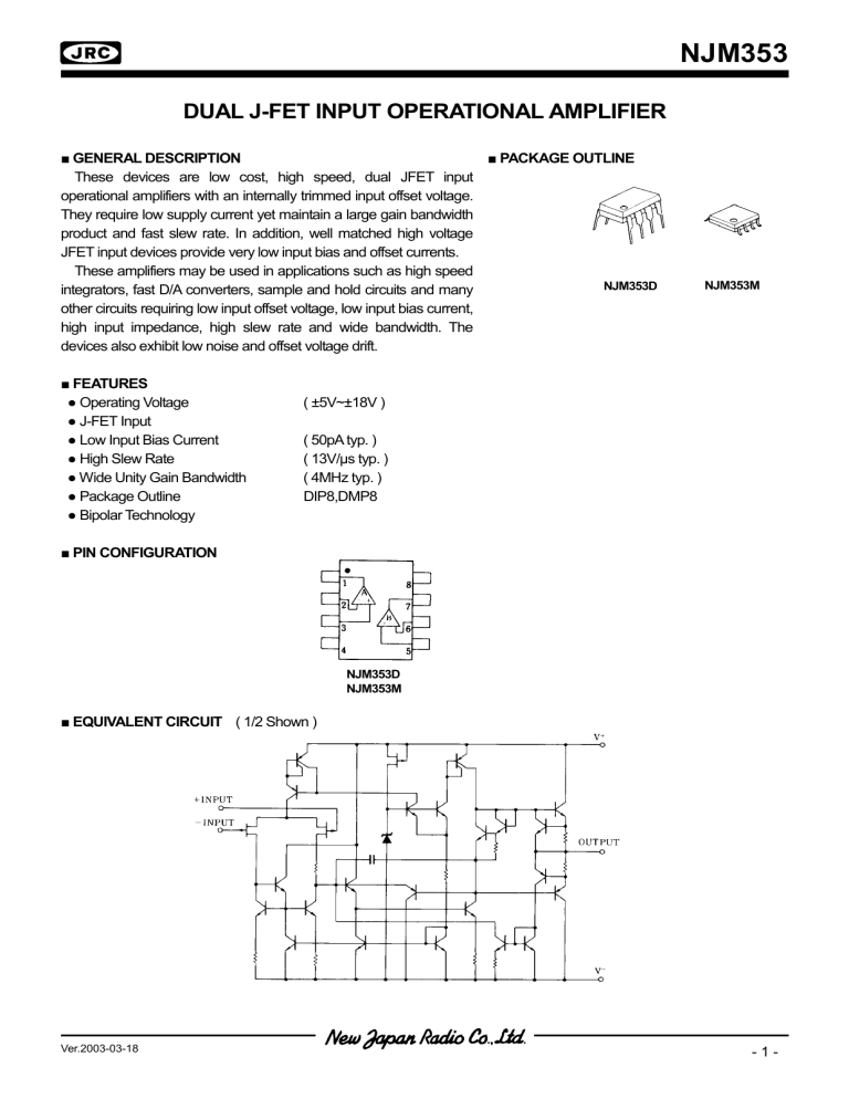
NJM353 DUAL J-FET INPUT OPERATIONAL AMPLIFIER ■ GENERAL DESCRIPTION ■ PACKAGE OUTLINE These devices are low cost, high speed, dual JFET input operational amplifiers with an internally trimmed input offset voltage. They require low supply current yet maintain a large gain bandwidth product and fast slew rate. In addition, well matched high voltage JFET input devices provide very low input bias and offset currents. These amplifiers may be used in applications such as high speed NJM353D integrators, fast D/A converters, sample and hold circuits and many other circuits requiring low input offset voltage, low input bias current, high input impedance, high slew rate and wide bandwidth. The devices also exhibit low noise and offset voltage drift. ■ FEATURES ● Operating Voltage ● J-FET Input ● Low Input Bias Current ● High Slew Rate ● Wide Unity Gain Bandwidth ● Package Outline ● Bipolar Technology NJM353M ( ±5V~±18V ) ( 50pA typ. ) ( 13V/µs typ. ) ( 4MHz typ. ) DIP8,DMP8 ■ PIN CONFIGURATION NJM353D NJM353M ■ EQUIVALENT CIRCUIT ( 1/2 Shown ) Ver.2003-03-18 -1- NJM353 ■ ABSOLUTE MAXIMUM RATINGS ( Ta=25˚C ) PARAMETER Supply Voltage Differential Input Voltage Input Voltage SYMBOL + V /V VID VIC Power Dissipation PD Operating Temperature Range Storage Temperature Range Topr Tstg RATINGS ± 18 ± 30 ± 15 ( DIP8 ) 500 ( DMP8 ) 300 -40~+85 -40~+125 UNIT V V V mW ˚C ˚C ( note ) For supply voltage less than ±15V. the absolute maximum input voltage is equal to the supply voltage. ■ ELECTRICAL CHARACTERISTICS ( Ta=25˚C,V+/V-=±15V ) PARAMETER Input Offset Voltage Average TC of Input Offset Voltage Input Offset Current Input Bias Current Input Resistance Large-signal Voltage Gain Maximum Peak-to peak Output Voltage Swing Input Common Mode Voltage Range Common Mode Rejection Ratio Supply Voltage Rejection Ratio Operating Current Channel Separate Slew Rate Unity Gain Bandwidth Equivalent Input Noise Voltage Equivalent Input Noise Current -2- SYMBOL VIO ∆VIO/∆T IIO IB RIN AV VOM VICM CMR SVR ICC CS SR fT en in TEST CONDITION RS=10kΩ RS=10kΩ RL=2kΩ,VO=±10V RL=10kΩ RS≤10kΩ f=1Hz~20kHz RS=100Ω,f=1kHz f=1kHz MIN. 88 ± 12 ± 11 70 70 - TYP. 5 10 25 50 12 10 100 ± 13.5 +15,-12 100 100 3.6 120 13 4 16 0.01 MAX. 10 100 200 6.5 - UNIT mV µV/˚C pA pA Ω dB V V dB dB mA dB V/µs MHz nV/√Hz pA/√Hz Ver.2003-03-18 NJM353 ■ TYPICAL CHARACTERISTICS Ver.2003-03-18 -3- NJM353 ■ TYPICAL CHARACTERISTICS -4- Ver.2003-03-18 NJM353 ■ TYPICAL CHARACTERISTICS Ver.2003-03-18 -5- NJM353 ■ TYPICAL CHARACTERISTICS [CAUTION] The specifications on this databook are only given for information , without any guarantee as regards either mistakes or omissions. The application circuits in this databook are described only to show representative usages of the product and not intended for the guarantee or permission of any right including the industrial rights. -6- Ver.2003-03-18


