FE55-0005 - Datasheet.Support
advertisement

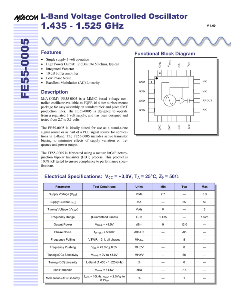
L-Band Voltage Controlled Oscillator Features VCC N/C N/C 1 GND N/C GND RF OUT GND N/C The FE55-0005 is ideally suited for use as a stand-alone signal source or as part of a PLL signal source for applications in L-Band. The FE55-0005 includes active transistor biasing to minimize effects of supply variation on frequency and power output. N/C M/A-COM's FE55-0005 is a MMIC based voltage controlled oscillator available as FQFP-16 4 mm surface mount package for easy assembly on standard pick and place SMT production lines. The FE55-0005 is designed to operate from a regulated 3 volt supply, and has been designed and tested from 2.7 to 3.3 volts. GND GND Description 16 GND Single supply 3 volt operation High Power Output: 12 dBm into 50 ohms, typical Integrated Varactor 10 dB buffer amplifier Low Phase Noise Excellent Modulation (AC) Linearity VTUNE Functional Block Diagram GND · · · · · · V 1.00 GND FE55-0005 1.435 - 1.525 GHz The FE55-0005 is fabricated using a mature InGaP heterojunction bipolar transistor (HBT) process. This product is 100% RF tested to ensure compliance to performance specifications. Electrical Specifications: VCC = +3.0V, TA = 25°C, Z0 = 509 Parameter Test Conditions Units Min Typ Max Supply Voltage (VCC) Volts 2.7 — 3.3 Supply Current (ICC) mA — 35 50 Tuning Voltage (VTUNE) Volts 0 — 3 Frequency Range (Guaranteed Limits) GHz 1.435 — 1.525 Output Power VTUNE = +1.5V dBm 9 12.0 — Phase Noise fOFFSET = 50kHz dBc/Hz — -85 — Frequency Pulling VSWR = 3:1, all phases MHzPP — 8 — Frequency Pushing VCC = +3.0V + 0.3V MHz/V — 8 — Tuning (DC) Sensitivity VTUNE = 0V to +3.0V MHz/V — 56 — Tuning (DC) Linearity L-Band (1.435 - 1.525 GHz) % — 6 — 2nd Harmonic VTUNE = +1.5V dBc — -15 — Modulation (AC) Linearity fMOD = 10kHz, vMOD = 2.5VPP to 0.1VPP % — 1 — L-Band Voltage Controlled Oscillator FE55-0005 V 1.00 Absolute Maximum Ratings 1,2 1. 2. +5 V Operating Temperature -40°C to +85°C Storage Temperature -65°C to +150°C VCC VCC VTUNE Absolute Maximum 100nH Parameter Recommended Bias Configuration 3,4 0.1µF 0.1µF 1000pF 16 Exceeding any one or a combination of these limits may cause permanent damage. Adequate DC and RF grounding required on board. 1 Pin Configuration RF OUT Pin No. Pin Name Function 1 GND Ground 2 GND Ground 3 GND Ground 4 GND Ground 5 GND Ground 6 GND Ground 7 GND Ground 8 N/C No Connect 9 N/C No Connect 10 RF Out RF Output 11 N/C No Connect 12 N/C No Connect 13 VCC Supply Voltage 14 N/C No Connect 15 VTUNE Tuning Voltage 16 GND Ground M/A-COM Inc. and its affiliates reserve the right to make changes to the product(s) or information contained herein without notice. M/A-COM makes no warranty, representation, or guarantee regarding the suitability of its products for any particular purpose, nor does M/A-COM assume any liability whatsoever arising out of the use or application of any product(s) or information. Visit www.macom.com for additional data sheets and product information. 3. 4. n n n For optimum performance, VCC bypass capacitors should be placed as close to the VCC lead as possible. For optimum performance, the VTUNE inductor should be placed as close to the VTUNE lead as possible. North America: Tel. (978) 442-4088 Asia/Pacific: Tel.+81-44-844-8296, Fax +81-44-844-8298 Europe: Tel. +44 (1908) 574 200, Fax+44 (1908) 574 300 2 L-Band Voltage Controlled Oscillator FE55-0005 V 1.00 Typical Performance Curves (VCC = +3.0V and VTUNE = +1.5V except where noted) Frequency vs. Tuning Voltage Frequency vs. Supply Voltage 1.508 TA = +85°C 1.53 FREQUENCY (GHz) FREQUENCY (GHz) 1.57 1.49 1.45 TA = -40°C 1.41 TA = +25°C 0.5 TA = +25°C 1.500 1.496 1.492 TA = -40°C 1.488 1.37 0.0 TA = +85°C 1.504 1.0 1.5 2.0 2.5 2.70 3.0 2.85 VTUNE (V) 3.30 15 OUTPUT POWER (dBm) OUTPUT POWER (dBm) 15 13 11 9 TA = -40°C 7 TA = +25°C TA = +85°C 0.0 0.5 1.0 1.5 2.0 2.5 13 11 9 7 TA = -40°C TA = +25°C TA = +85°C 5 5 2.70 3.0 2.85 3.00 3.15 3.30 VCC (V) VTUNE (V) Supply Current vs. Supply Voltage Supply Current vs. Tuning Voltage 45 TA = -40°C TA = -40°C SUPPLY CURRENT (mA) SUPPLY CURRENT (mA) 3.15 Output Power vs. Supply Voltage Output Power vs. Tuning Voltage 45 3.00 VCC (V) 40 35 30 25 TA = +25°C 40 35 30 25 TA = +25°C TA = +85°C TA = +85°C 20 20 0.0 0.5 1.0 1.5 2.0 2.5 2.7 3.0 Visit www.macom.com for additional data sheets and product information. 3 3.15 3.3 VCC (V) VTUNE (V) M/A-COM Inc. and its affiliates reserve the right to make changes to the product(s) or information contained herein without notice. M/A-COM makes no warranty, representation, or guarantee regarding the suitability of its products for any particular purpose, nor does M/A-COM assume any liability whatsoever arising out of the use or application of any product(s) or information. 2.85 n n n North America: Tel. (978) 442-4088 Asia/Pacific: Tel.+81-44-844-8296, Fax +81-44-844-8298 Europe: Tel. +44 (1908) 574 200, Fax+44 (1908) 574 300 3 L-Band Voltage Controlled Oscillator FE55-0005 V 1.00 Ordering Information Part Number Package FE55-0005 FQFP-16 4mm Package Outline Drawing M/A-COM Inc. and its affiliates reserve the right to make changes to the product(s) or information contained herein without notice. M/A-COM makes no warranty, representation, or guarantee regarding the suitability of its products for any particular purpose, nor does M/A-COM assume any liability whatsoever arising out of the use or application of any product(s) or information. Visit www.macom.com for additional data sheets and product information. n n n North America: Tel. (978) 442-4088 Asia/Pacific: Tel.+81-44-844-8296, Fax +81-44-844-8298 Europe: Tel. +44 (1908) 574 200, Fax+44 (1908) 574 300 4


