Clifton Laboratories
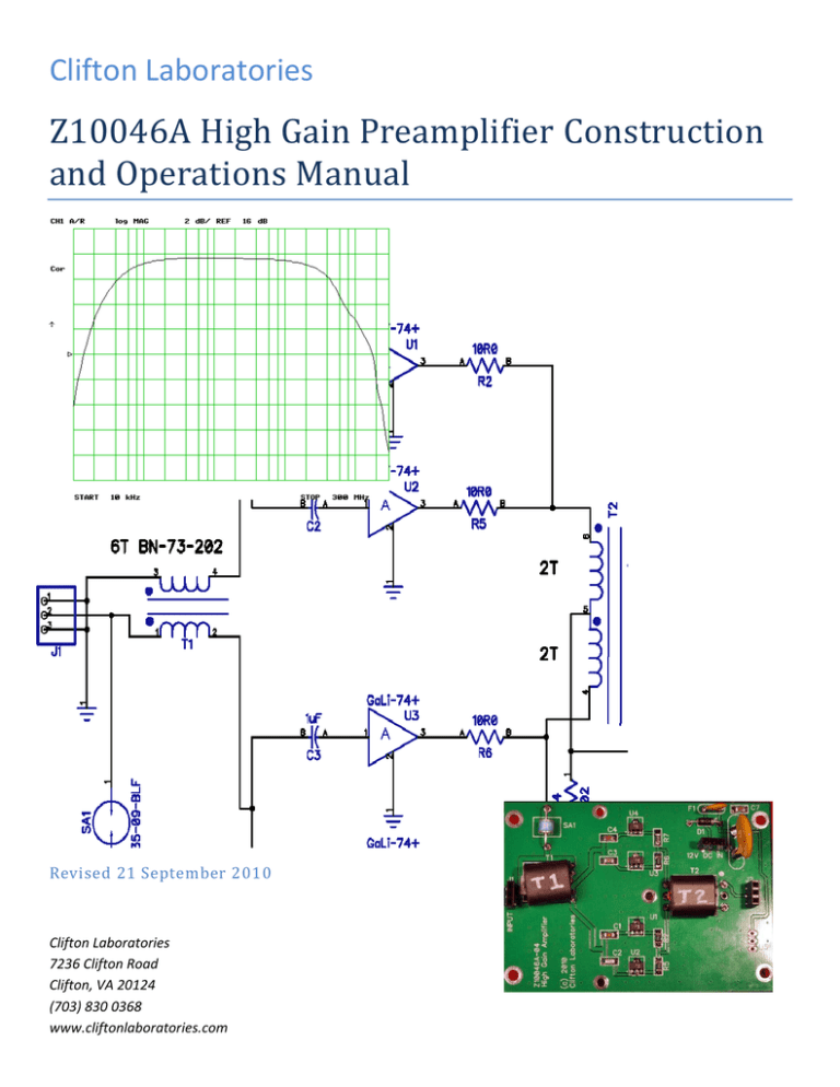
Z10046A High Gain Preamplifier Construction
and Operations Manual
Revised 21 September 2010
Clifton Laboratories
7236 Clifton Road
Clifton, VA 20124
(703) 830 0368
www.cliftonlaboratories.com
Model Z10046A High Gain Amplifier
Revised 21 September 2010
(c) 2010 Jack R. Smith d/b/a/ Clifton Laboratories.
Trademarks and Copyright
Material in this document copyrighted © 2009, 2010 Clifton Laboratories. All rights reserved. It is provided to allow the
Z10046A purchasers to maintain their equipment and such other purposes as may not be prohibited by law.
Warranty
This warranty is effective as of the date of first consumer purchase.
What is covered: During the ninety (90) days after date of purchase, Clifton Laboratories will correct any defects in the
Z10046A due to defective parts (kit or assembled) or workmanship (if purchased as an assembled unit) free of charge
(post-paid). You must send the unit at your expense to Clifton Laboratories, but we will pay return shipping. Clifton
Laboratories’ warranty does not extend to defects caused by your incorrect assembly or use of unauthorized parts or
materials or construction practices.
What is not covered: If the Z10046A is purchased as a kit, this warranty does not cover correction of assembly errors or
misalignment; repair of damage caused by misuse, negligence, or builder modifications; or any performance
malfunctions involving non-Clifton Laboratories accessory equipment. The use of acid-core solder, water-soluble flux
solder, or any corrosive or conductive flux or solvent will void this warranty in its entirety. Whether purchased as an
assembled unit or as a kit, also not covered is reimbursement for loss of use, inconvenience, customer assembly or
alignment time, or cost of unauthorized service. Damage due to operating the Z10046A near a transmitting antenna is
not covered under the warranty.
Limitation of incidental or consequential damages: This warranty does not extend to non-Clifton Laboratories
equipment or components used in conjunction with our products. Any such repair or replacement is the responsibility of
the customer. Clifton Laboratories will not be liable for any special, indirect, incidental or consequential damages,
including but not limited to any loss of business or profits.
Under no circumstances is Clifton Laboratories liable for damage to your equipment connected to the Z10046A
resulting from use of the Z10046A, whether in accordance with the instructions in this Manual or otherwise.
Z10046A Construction and Operations Manual
Page 1
Table of Contents
Model Z10046A High Gain Amplifier ...................................................................................................................................... 1
Specifications .......................................................................................................................................................................... 3
Overview ............................................................................................................................................................................. 3
Typical Measured Performance Plots ................................................................................................................................. 4
Frequency Response ....................................................................................................................................................... 4
Noise Figure .................................................................................................................................................................... 4
1 dB Compression Point and Saturated Output Power .................................................................................................. 4
Input SWR ....................................................................................................................................................................... 4
OIP as Function of Idle Current ....................................................................................................................................... 5
Assembly ................................................................................................................................................................................. 6
R1, R2 and R4 selection. .................................................................................................................................................. 6
T1 and T2 Turns Ratio ..................................................................................................................................................... 6
Component Location (bottom and top) ......................................................................................................................... 7
Recommended Assembly Order ......................................................................................................................................... 7
Printed Circuit Board Assembly ...................................................................................................................................... 7
Completed Z10046A View............................................................................................................................................. 15
Board Size and Mounting Hole Locations ..................................................................................................................... 17
Theory of Operation.......................................................................................................................................................... 18
Troubleshooting ................................................................................................................................................................ 20
Resistance Readings ...................................................................................................................................................... 21
Voltage Readings ........................................................................................................................................................... 22
Parts List ................................................................................................................................................................................ 23
Z10046A Construction and Operations Manual
Page 2
Specifications
Plots in this Manual are taken from production units but demonstrate typical, not warranted, performance. Clifton
Laboratories offers an optional measured performance data for any Z10046A amplifier. Contact Clifton Laboratories for
price and availability of measured data.
Overview
Parameter
Dimensions
DC Supply
Gain
Frequency Range
Intermodulation [2]
1 dB Compression
Point
Input SWR
Isolation (reverse
gain)
Value
The Z10046A printed circuit board is 3.5 inches x 2.5 inches (88.9mm x 63.5mm).
Recommend minimum enclosure height is 1.5 inches (38.1 mm).
The Z10046A requires 10.0V at a current (depending upon user selected bias resistor
options) from 320 mA to 400 mA. A suitable 10.0V regulator is supplied with the Z10046A
and can be used with supply voltages of 12.5V to 20V. Proper heat sinking of the 10V
regulator is required.
23.5 dB nominal at 1 MHz
-3 dB points are 50 KHz – 50 MHz [1]
Both second and third order output intercepts depend upon selected bias resistor
options. OIP2 is typically +87 to +93 dBm; OIP3 is typically +42 dBm to +45 dBm.
+24.7 dBm output at 1 MHz.
Less than 1.5:1, 300 KHz-30 MHz
Typically 30 dB at 1 MHz
[1] Frequency response based upon standard transformer ratio of T1=6:6 turns, T2=2:2:4 turns. For improved lower
frequency response, T1 may be increased to 7 turns and T2 wound as 3:3:6 turns. With these changes, the -3 dB points
become 15 KHz and 40 MHz. Unless otherwise stated, performance data is for standard turns ratio.
[2] Intermodulation measured with test tones of 3007 KHz and 4011 KHz, adjusted for 0 dBm output (each tone) after 30
minute thermal stabilization period. Second order intercept is a function of amplifier balance which is dependent, to
some degree, upon the care the builder takes in construction and upon the PCB’s thermal balance. See plot of typical
OIP2/OIP3 as function of idle current later in this manual.
Z10046A Construction and Operations Manual
Page 3
Typical Measured Performance Plots
Frequency Response
Noise Figure
1 dB Compression Point and Saturated Output
Power
Input SWR
Z10046A Construction and Operations Manual
Page 4
OIP as Function of Idle Current
Test conditions: Test tones of 1007 KHz and 4011 KHz, adjusted in level to achieve 0 dBm output (per tone). Supply
voltage adjusted to vary idle current.
Z10046A Construction and Operations Manual
Page 5
Assembly
R1, R2 and R4 selection.
The Z10046A uses four Mini-Circuits GaLi-74+ amplifier modules in parallel push-pull. The GaLi-74’s bias current is
determined by the series resistor string of R1, R3 and R4. Increased bias (lower value R1, R3 and R4) improves
intermodulation distortion performance, but increases current drain and device temperature. The typical per device bias
range runs from 80 mA to 100 mA, with 80 mA being the “recommended” current level and 130 mA being the maximum
current rating.
When purchased, the Z10046A is shipped with bias resistors of one of three values:
Bias Resistor Value*
(ohms)(R1, R3 & R4)
4.02
3.32
3.01
Nominal Idle Current per
device w/ 10V supply (mA)
80
90
100
Typical OIP2
(dBm)
+87
+90
+93
Typical OIP3
(dBm)
+43
+45
+46
Typical Tmax (degrees
F/C) PCB in open air
+131F/55
+134F/57
+140F/61
*Resistor value assumes series RF choke of 2.0 ohms is inserted between 10.0V regulator output and R1, R3 and R4
string.
Unless the particular application requires maximum intermodulation intercepts, Clifton Laboratories recommends 4.02
ohms for R1, R3 and R4, corresponding to 80 mA/device. Although higher bias current improves performance, increased
operating temperature will reduce component life. (There is some unit-to-unit variation in idle current, OIP2, OIP3and
Tmax. The values in the table are representative, but are not guaranteed.)
T1 and T2 Turns Ratio
If improved performance below 50 KHz is required, and if some loss in gain above 30 MHz is acceptable, T1 and T2 may
be modified with additional turns.
Transformer
T1
T2
Turns Ratio
6 turns bifilar
2 turns bifilar & 4
turns single wire
Standard Design
Response
-1 dB
-2 dB
57 KHz33 MHz
38 KHz48 MHz
-3 dB
27 KHz61 MHz
Extended Low Frequency Performance
Response
Turns Ratio
-1 dB
-2 dB
-3 dB
7 turns bifilar
32 KHz20 KHz15 KHz3 turns bifilar & 6
28.8 MHz
39.2 MHz
>40 MHz
turns single wire
Sufficient wire is provided for either the standard design or the extended low frequency performance design.
Z10046A Construction and Operations Manual
Page 6
Component Location (bottom and top)
Z10046A Copper Foil Thickness. The Z10046A PCB is constructed with copper thickness three times that of a
typical PCB. This is done to aid thermal tracking of U1-U4, necessary for best 2nd order intermodulation performance.
From the prospective of the builder, the extra copper thickness requires a larger soldering iron and possibly a higher
temperature setting than used for normal printed circuit board assembly, particularly when soldering ground pads.
Recommended Assembly Order
Printed Circuit Board Assembly
Bottom PCB Surface
Note: RV2 is not used.
Install C19, a 10uF capacitor, marked 10 EHA. The negative
terminal of C19 is identified by the black stripe. Observe
polarity when installing C19. If you have it, a small amount of
electronics grade solder flux can be applied to C19’s pads.
I used a spring clothespin, with one side cut into a “V” shape
hold small parts in place while soldering.
liquid
to
Install C9, a 1uF ceramic capacitor. This component is not marked.
Install C10, a 10pF ceramic capacitor. This component is not marked.
Install R1, R3 and R4. The value of these three resistors depends upon the idle current option ordered at
time of purchase. Possible values are 4.02 ohms (marked 4R02), 3.32 ohms (marked 3R32) and 3.01
ohms (marked 3R01).
Z10046A Construction and Operations Manual
Page 7
Perform a resistance and continuity check.
From TP1 and TP2 to ground should be high impedance. These
points have only leakage resistance of C19 which will normally
the 1 megohm or greater range.
Between TP1 and TP2 should be the sum of R1, R3 and R4. This
particular resistance will thus depend upon the selected values
R1, R3 and R4.
two
be in
for
Top PCB Surface
Wind transformers T1 and T2
T1 and T2 are wound on multi-aperture (binocular)
When counting turns, remember that one turn requires
to pass through both holes. The photo at right shows
complete turn through a binocular core. Passing the
through one hole counts as one-half of a turn.
cores.
the wire
one
wire
Notes in winding T1 and T2
T1 and T2 are ferrite cores and have sharp edges. To avoid wire damage caused by abrading the
enamel insulation during winding, Teflon insert bushings are used..
The magnet wire supplied with the Z10046A is “solder strippable” which means that the
insulation will dissolve in molten solder. First wind the transformer and after winding clamp the
transformer in place with a soft jaw vise. Cut the lead length to the recommended value and
apply the soldering iron to the wire end. Add solder to form a ‘blob’ of molten solder. After a
few seconds, the insulation will begin to dissolve. Work the soldering iron along the wire, adding
fresh solder as necessary to maintain a blob of molten solder. Do not tin right up to the core; tin
only to within 1/8th inch (3mm) of the core.
Z10046A Construction and Operations Manual
Page 8
Cut four bushings from the
length of Teflon tubing. The
bushings should slightly
extend (between 1/16th and
1/32nd inch [1.5mm to
0.75mm]) from each end of
core when inserted.
When cutting the Teflon
tubing, use a sharp hobby
or a razor blade. Scissors or
wire cutters can leave a
ragged edge. After cutting,
the tubing between your
fingers to restore it to circularity.
the
knife
dull
roll
The tubing more or less “self centers” lengthwise if you
wind 1.5 turns of bifilar wire and gently pull the wire
first
ends.
[Many of the photos in this manual show a transformer
wound without a Teflon bushing. The photographs will
updated in a later edition of this Manual.]
be
The instructions for T1 below assume standard frequency response is desired. If extended low frequency
response is desired, and some loss in high frequency response is acceptable, use the alternative winding
ratios provided under the section T1 and T2 Turns Ratio. T1 will require 7 turns if extended low
frequency response option is impelemnted. In this case T1’s wire length will be 14 inches (350mm).
T1: Cut lengths of no. 30 red and no. 30 green magnet wire
inches (300mm) long. Twist the red and green wires
together with approximately 45 turns. (40 to 50 turns is OK.)
Install Teflon bushings in both core holes and wind the
twisted wire through the core with 6 turns. When starting
winding, allow approximately one inch (25mm) of wire to
extend from one hole.
12
the
After winding six turns, trim both twisted pair ends to
extend approximately ¾ inch (18 mm) from the core end. Untwist the extended wires and tin using the
procedure summarized above.
Set T1 aside.
Z10046A Construction and Operations Manual
Page 9
The instructions for T2 below assume standard frequency response is desired. If extended low frequency
response is desired, and some loss in high frequency response is acceptable, use the alternative winding
ratios provided under the section T1 and T2 Turns Ratio. T1 will require 3 bifilar turns and 6 standard
turns if extended low frequency response option is impelemnted. In this case T1’s wire length will be 10
inches (250mm) for the bifilar winding and 12 inches (300mm) for the single wire winding.
T2: Cut lengths of no. 30 red and no. 30 green magnet wire 8 inches (200 mm) long. Twist the red and
green wires together approximately 30 turns (25 to 35 turns is OK.)
Install Teflon bushings in both core holes and wind two turns through the core. When starting the
winding, allow approximately one inch (25mm) of wire to extend from one hole.
After winding two turns, trim both twisted end pairs to extend approximately ¾ inch (18 mm) from the
core end. Untwist the extended wires. Both holes have red and green wires. Twist the red wire from one
hole with the green wire from the other hole. This will yield a winding with three leads, as illustrated
conceptually at the right.
Cut a length of red no. 30 magnet wire 10 inches (250 mm)
long.
Starting at the opposite end (the end that does not have
extending from it), wind four turns on the core. Allow
approximately one inch (25 mm) of wire to extend when
starting the winding.
leads
When winding the four turns, it helps to bend the first
winding leads against the side of the transformer core.
Cut the leads to approximately ¾ inch (16 mm) and tin. The
completed transformer should match the photo below.
Set T2 aside for later installation.
Install C1, C2, C3, C4 and C7, 1uF capacitors. These have no markings.
Install R2, R5, R6 and R7, 10.0 ohm resistors, marked 10R0.
Install U1, U2, U3 and U4, Gali-74+ devices, marked 74.
If you have liquid electronic grade soldering flux, apply a small amount to U1-U4 pads.
When installing U1-U4, I lightly tin one of the outside pads and slide the device into place while heating
the pad with a soldering iron. When the device is aligned with the pad, remove the soldering iron and
allow it to cool.
Z10046A Construction and Operations Manual
Page 10
Solder the remaining pins and the large tab at the rear of the device. To reduce the risk of overheating
the devices I normally solder the other outside pin of each device and then the center pins of each
device and lastly the tab of each device. (Outside pin U1, outside pin U2, outside pin U3, outside pin U4,
then center pin U1, center pin U2, etc.)
Note that these devices may be difficult to install as the Z10046A’s thicker copper foil wicks away heat,
particularly if the soldering iron has a small diameter tip.
Cut two lengths ½ inch long (12 mm) of ¼ inch (6 mm) wide
double side adhesive foam tape. Apply the tape to hold T1 and
place as illustrated.
T2 in
Remove the protective paper from the foam at T1 and install T1 as illustrated in the photo below.
The red and green wires from each hole go to the two pads
to the outside of the hole.
closest
When pulling the leads through the hole, do not pull the
tight against the core. Rather allow the leads to extend
horizontally from the core and then bend downwards at a
degree angle. This will reduce the risk of abrading the wire
the core edges.
wires
90
against
Remove the protective paper from the
at T2 and install T2 as illustrated at the
foam
right.
When pulling the leads through the
do not pull the wires tight against the
Rather allow the leads to extend
horizontally from the core and then
downwards at a 90 degree angle. This
reduce the risk of abrading the wire against the core edges.
hole,
core.
bend
will
Install 3-pin header sockets at J1, J2 and J3 and on the PCB at U5.
Install the spark gap at SA1. This part is marked 90V. Space the spark gap approximately 1/8th inch
(3mm) above the top surface of the printed circuit board.
Install the 500 mA polyfuse at F1. This part is marked XF050.
Install the over-voltage MOV at RV1. This part is marked 180M.
Install diode D1. This part will be of the 1N400x family where X is a number from 1 to 7 and it will be
marked as such. When installing D1, observe polarity; the band on the diode should be oriented to
Z10046A Construction and Operations Manual
Page 11
match the line marking on D1’s silk screen outline.
With an ohmmeter check the resistance to ground of TP2. It should not show a low resistance to ground.
(Anything above 400 ohms is OK.)
With an ohmmeter check the resistance to ground of the center pin of J1. It should be greater than 10K.
In theory, both resistance checks should be in the mega-ohm range. However, if the windings of T1 or T2
are abraded, the windings will form a medium resistance connection to T1 or T2’s core. (If you place the
ohmmeter probes touching T1 or T2’s core, you will measure a resistance in the 10 to 50 Kohm range,
depending on size of the probe, pressure, etc.) Moveover, ohmmeters differ in the open circuit voltage
they apply which can cause wildly different readings if one ohmmeter does not bias semiconductor
junctions into conductivity but a second ohmmeter does.
No leakage should be observed between the primary and secondary windings if you have used Teflon
bushings.
Checkout with laboratory adjustable voltage power supply
If you have an adjustable voltage, current limited power supply, set it at 10.00 volts, with current
limiting at 450 mA.
DO NOT EXCEED 10.250 VOLTS OR DAMAGE MAY OCCUR TO U1-U4.
The DC resistance of RF choke L1 (approximately 2 ohms) is part of the current limiting
resistance. When making the test described below temporarily connect L1 between the adjustable
power supply positive output and the U5 +10V PCB pad.
Connect the power supply to U5’s socket as illustrated.
Observe the current draw. If it significantly exceeds the expected
(four times the individual GaLi-74 current draw based upon your
selection of bias resistors), disconnect the power supply and
troubleshoot the Z10046A.
level
For the resistor values supplied with the Z10046A, the current draw
in the range 300 mA to 425 mA. Values outside this range should be
investigated.
will be
If the current draw appears correct, measure the current through U1-U4. To do this, measure the
voltage drop across R2, R5, R6 and R7 (10.0 ohm resistors) and calculate the current in mA by dividing
voltage drop by the resistance, 10 ohms. For example, if R2 has a voltage drop of 0.823 volts, U1’s
current draw is 0.823/10 = 82.3 mA.
U1-U4 should have quite similar current draws. Investigate any significant difference in current draw
amongst U1-U4. (Typically the maximum difference is 3 or 4 mA.) The current draw will change as U1-U4
warm up and stabilize in temperature, and the most accurate readings will be obtained after a 10 or 15
minute temperature stabilization period.
Z10046A Construction and Operations Manual
Page 12
Checkout without a variable power supply.
If you do not have a variable voltage power supply, it is necessary to use the 10.0V regulator supplied
with the Z10046A as the 10.0V power source.
U5 – 10.0V Regulator.
U5 is a 10.0V precision
voltage regulator supplied
the Z10046A and intended to
part of the completed
amplifier.
U5 will dissipate several watts
power and must be
adequately heat sinked.
Normally mounting U5 to the
enclosure housing the
Z10046A will provide
adequate heat sinking.
with
be
of
In order to maintain the
lowest feasible temperature
gradient across U1-U4, U5 should be mounted along the center line of the printed circuit board and on
the outside of the PCB. In order to avoid unwanted parasitic oscillations, the leads between U5 and the
PCB should not exceed 2 inches (50mm).
The illustration at the right shows U5 installed in the Clifton Laboratories enclosure. Note that U5 is
approximately centered and mounted approximately 0.5 inch (12mm) beyond the PCB edge.
Cut lengths of red and black wire to 2 inches (50mm). Strip both ends of each wire approximately 3/16th
inch (5mm) and tin. Locate the 1 mH RF choke (Marked 5800-102) and trim the leads so that the choke
body is centered and the overall length is 2 inches (50mm). Cut lengths of small diameter (1/16th inch or
1.5mm) blue heat shrink tubing and slide over the RF choke’s leads. Approximately 1/8 inch (3mm) of
the wire should be exposed at the ends. Apply heat to shrink the blue tubing.
Wire a 3-pin header socket with red and black wires and the RF choke as shown below. Slip lengths
(approximately ¼ inch (6mm)) of red, black and blue shrink tubing over the associated color wire (or,
choke lead for the blue tubing) before making the solder connection. After the socket is soldered in
place, slide the tubing over the joint and apply heat to shrink.
Slip a short length of heat
tubing (red for the red wire
black for the black wire) over
wire ends. Solder the red and
wires to a three pin header,
not attach the blue lead from
choke. Follow the illustration
Z10046A Construction and Operations Manual
shrink
and
the
black
but do
the RF
at the
Page 13
right. Slide the shrink tubing over the joints and apply heat to shrink.
Plug the pin header into the printed circuit board socket at U5 following the polarity shown in the
drawing at the right.
The
photo
shows an assembled jumper. I twisted the
wires
together as a matter of neatness; it is not
electrically necessary.
Mount U5 using 4-40 hardware (supplied with the Z10046A) and attach the 3-pin header socket to U5. It
may be a tight fit to push the socket over the pins. Orient the socket as shown in the illustrations.
Apply +13.8V to J3, DC Power in. J3’s center pin
in; the two outside pins are ground. Either or
outside pins may be used.
is DC
both
Measure U5’s output voltage (RF choke with blue
shrink). It should be within the range 9.75V to
10.25V.
heat
If U5’s output voltage is within this range,
remove the header pin from the PCB socket.
Remove DC input power and slip a short length of blue shrink tubing over the RF choke’s free end lead.
Solder to the remaining header pin. Slide the shrink tubing over the solder joint and apply heat to shrink.
.
Reapply 13.8V to J3. Observe the current draw. If it significantly exceeds the expected level (four times
the individual GaLi-74 current draw based upon your selection of bias resistors), disconnect the power
supply and troubleshoot the Z10046A.
For the resistor values supplied with the Z10046A, the current draw will be in the range 300 mA to 425
mA. Values outside this range should be investigated.
If the current draw appears correct, measure the current through U1-U4. To do this, measure the
voltage drop across R2, R5, R6 and R7 (10.0 ohm resistors) and calculate the current in mA by dividing
voltage drop by the resistance, 10 ohms. For example, if R2 has a voltage drop across it of 0.823 volts,
U1’s current draw is 0.823/10 = 82.3 mA.
U1-U4 should have quite similar current draws. Investigate any significant difference in current draw
amongst U1-U4. (Typically the maximum difference is 3 or 4 mA.) The current draw will change as U1-U4
warm up and stabilize in temperature, and the most accurate readings will be obtained after a 10 or 15
minute temperature stabilization period.
Measure the voltage at the output pin of U1-U4. Record the voltage and current in the table below.
Z10046A Construction and Operations Manual
Page 14
Device
U1
U2
U3
U4
Current (mA)
Voltage (Volts)
Completed Z10046A View
Z10046A Construction and Operations Manual
Page 15
Z10046A Construction and Operations Manual
Page 16
Board Size and Mounting Hole Locations
Mounting holes are for 4-40 hardware (0.125 inch / 3.2mm diameter). DO NOT USE THE THREE SMALLER HOLES TO
MOUNT THE BOARD.
Z10046A Construction and Operations Manual
Page 17
Theory of Operation
The Z10046A comprises four Mini-Circuits GaLi-74+ Monolithic Microwave Integrated Circuit (MMIC) amplifiers, U1-U4.
The GaLi-74 amplifiers have 50 ohms input and output impedance and a typical gain of 25.1 dB, with OIP3 of +38 dBm
and a 1 dB compression point (output) of +19 dBm. The GaLi-74’s lower frequency limit is determined by the input
coupling circuit, and the upper -3 dB point is 1 GHz. The noise figure is 2.7 dB.
Although a single GaLi-74 provides reasonable performance, it is possible to improve certain critical parameters by
operating multiple devices. Paralleling two GaLi-74’s results in an input and output impedance of 25 ohms. If this parallel
combination is operated in push-pull, the input and output impedance is the sum of the push pull sections, or 50 ohms.
Thus, four devices in parallel – push-pull provides a convenient 50 ohm input and output impedance. Since the signal is
shared equally amongst four amplifiers, the output 1 dB compression point will improve approximately 6 dB over a
single amplifier. Likewise, OIP3 will improve approximately 6 dB. Noise figure will remain unchanged, as does the
frequency response.
In order to convert the 50 ohm unbalanced input (J1) to balanced 50 ohm drive to the push-pull sections, a 1:1 balun is
used. T1 is 6 bifilar turns on a Fair-Rite 73 material core, and provides acceptable unbalanced-to-balanced
transformation over the frequency range 25 KHz – 60 MHz.
C1-C4 are DC blocking capacitors, as U1-U4 have DC voltage at their input pins.
The output 25 ohm amplifier sections are converted back to a single ended 50 ohm output by T2. In addition, T2
provides a convenient DC feed point.
The GaLi-74’s output is both an RF output and DC feed point. Mini-Circuits’ Application Note AN-60-010 provides the
following description of the biasing network required for proper operation of its line of MMICs:
Z10046A Construction and Operations Manual
Page 18
The internal circuit configuration is a Darlington pair, embedded in a
resistor network as shown in the schematic diagram, Figure 1.
Applying DC power to operate this kind of amplifier is simpler than
biasing a transistor. Like a discrete bipolar transistor, this circuit is
current-controlled rather than voltage-controlled. This means that for
a range of current around a recommended value, the device voltage
varies much less than in proportion to current. A constant-current DC
source would be ideal for providing a stable operating point. By
contrast, with most of these models the use of a constant-voltage DC source would cause the current to vary
widely with small changes in supply voltage, temperature change, and device-to-device variations. Stable
operating point needs an external series resistor between the amplifier and a DC voltage supply to approximate
a constant-current source.
The Z10046A approximates a constant current source as recommended by Mini-Circuits, a fixed voltage supply and a
series resistor. R1, R3 and R4, and the DC resistance of L1, form one part of the series resistor. However, simply
connecting U1-U4 to the output transformer pins all outputs at the same voltage and yields unequal current sharing
amongst the four devices. Small differences amongst U1-U4, either as a part of manufacturing tolerance or unequal
temperature among U1-U4, cause current unbalance and degrades second order intercept. Equalizing resistors R2, R5,
R6 and R7 permit U1-U4 to have slightly different terminal voltages and equalizes currents. 10 dB or more improvement
in OIP2 is provided by adding the four equalizing resistors. Approximately 2 dB gain is lost as a consequence of the
equalizing resistors.
L1, and the associated bypass capacitors, reduces broadband noise from U5, which would otherwise be coupled to the
Z10046A’s output. U5’s noise contribution is most objectionable below 500 KHz, and is reduced to negligible levels by L1
and the associated bypass.
DC input power is over-voltage clamped by an MOV, RV1 and is short circuit protected by a positive temperature
coefficient thermistor or Polyfuse, F1. Reverse voltage protection (in addition to that provided by U5) is accomplished by
D1. SA1 is a spark gap intended to fire in the event of gross overvoltage on the input. SA1 fires at 90 volts, so it will not
protect the Z10046A from damage, but is rather intended to reduce damage to equipment that might be connected to
the Z10046A in the event of a nearby lightning strike.
Z10046A Construction and Operations Manual
Page 19
Troubleshooting
Schematic diagrams are provided with typical voltage and resistance readings.
In troubleshooting the Z10046A, remember that the specific voltages on U1-U4 are a function of the bias resistor and
U5’s output voltage. In general, the most useful measurement technique, if U1-U4 are suspect, is to compare the
voltage and current for all four devices. U1-U4 voltages and currents will closely track and any significant divergence
should be investigated.
It is possible to measure individual bias current for U1-U4 by measuring the voltage drop across the associated 10R0
equalization resistors. The current in mA equals the drop across the 10R resistor (in millivolts) divided by 10.0.
T1 and T2 are Fair-Rite 73 material ferrite and exhibits finite resistance. Placing ohmmeter probes on either T1 or T2
material will read in the tens of thousands of ohms. If T1’s winding has abraded insulation, J1 resistance to ground will
not be the expected near open circuit, but will be in the low to medium kilo-ohm range. If the transformer has been
wound with Teflon sleeves, no such abrasion should occur and J1 should be near infinite resistance to ground. In most
instances, however, amplifier performance will not be significantly degraded even if T1 has abraded winding insulation.
U1-U4 normally run warm, with a power dissipation in the 0.5 watt range for each device. Bias current is affected by
temperature changes and it is normal to see a modest change in current consumption, on the order of 5% or less, from
cold start to fully temperature stabilized operation.
Optimum second order intermodulation product performance requires U1-U4 to be isothermal, i.e., no major
temperature difference from U1 to U4. The Z10046A PCB is designed to equalize temperature across U1-U4 under
normal circumstances. However, it is possible that where a Clifton Laboratories provided enclosure is not used, issues
related to thermal balance may occur. If 3rd order intermodulation performance is normal, but 2nd order intermodulation
is somewhat below standard, temperature differentials amongst U1-U4 should be examined. In general, achieving high
2nd order intermodulation performance requires a high order of balance amongst U1-U4 and associated components.
Hence, differential measurements among U1-U4 are a good way to approach troubleshooting.
Z10046A Construction and Operations Manual
Page 20
Resistance
Readings
Z10046A Construction and Operations Manual
Page 21
Voltage
Readings
Z10046A Construction and Operations Manual
Page 22
Parts List
The scale in the photograph is marked in inches and tenths of an inch (2.54mm).
Parts values in this manual are identified with the decimal point indicated by the multiplier digit. For example a 10.0
ohm resistor is identified as 10R0, a 1.0uF capacitor as 1u0, etc.
Photo
Component ID
Value
Marking
Quantity
C1,C2,C3,C4,C7,C
9
1uF, X7R, 50V
1206 ceramic
capacitor
10pF, NP0/C0G,
50V 1206 ceramic
capacitor
None
6
None
1
10 EHA
1
D1
10uF, 25V 105°C
electrolytic
capacitor
1N4007
1N4007
1
F1
500mA polyfuse
RXEF050S
1
J1,J2,J3 & J4; U5
socket (and U5
PCB socket)
3 position, 0.1
inch spacing
single row, 0.025
inch square pin
header socket
PINHD-1X3
6
R1, R3 & R4
1 watt, 2512 size
resistor; value as
determined by
customer’s
selection of idle
current.
Marking is nRnn where n is
a digit from 0 to 9 and R
indicates the decimal point.
4.02 ohms, for example, will
be marked 4R02.
3
C10
C19
Z10046A Construction and Operations Manual
Page 23
R2, R4, R5 & R6
10R0
10R0
4
RV1
18V MOV
180M
1
0.1 inch single row
12
Header Pins
(male)
SA1
2035-09-BLF
90V
1
T1, T2
BN-73-202
None
2
Z10046A Construction and Operations Manual
Page 24
U1, U2,U3,U4
GaLi-74+
74
4
U5
7810 threeterminal
regulator; -2%
tolerance or
better
Z10046A
Depends upon supplier;
part will have ‘7810’ in the
marking, e.g., KA7810AETU
1
Z10046A-X where X is the
PCB revision number
1
Printed Circuit
Board
None
Wire
Teflon Bushing
No. 30 red &
green
3 inches (75mm)
0.103 ID
24
L1
1 mH RF Choke
None
Hookup wire
Red wire
3
None
Hookup wire
Black wire
3
None
Shrink tubing
Blue small shrink
3
None
Shrink tubing
Black 1/8” shrink
1
None
Shrink tubing
Blue 1/8” shrink
1
None
Shrink tubing
Red 1/8” shrink
1
None
Foam tape,
double sided 1/4"
wide
Voltage regulator
screw
None
Approx. 1” (25mm)
long
None
Lockwasher
None
Flat washer
4-40 x 3/8"
PanHead Philips
18-8 SS
4-40 spring
lockwasher 18-8
SS
4-40 hole 18-8 SS
None
Small pattern nut
4-40 thd 18-8 SS
Z10046A Construction and Operations Manual
1
1
1
1
Page 25
