PS-2 - SG1524
SIMPLIFYING CONVERTER DESIGN WITH A
NEW INTEGRATED REGULATING PULSE
WIDTH MODULATOR
Abstract
A new monolithic integrated circuit is described which contains all the control circuitry for a regulating power supply converter or
switching regulator. Included in this 16-pin dual-in-line package is the voltage reference, error amplifier, oscillator, pulse width
modulator, pulse steering flip-flop, dual alternating output switches, and current limiting and shutdown circuitry. This device can
be used for switching regulators of either polarity, transformer coupled DC to DC converters, transformer-less voltage doublers
and polarity converters, as well as other power control applications.
Introduction
Implementing a switching power supply has just become
significantly easier with the introduction of the SG1524
series of Regulating Pulse Width Modulator integrated
circuits. Long recognized as offering greatly improved
efficiencies, the development of switching supplies has
been hampered by the complexity of the low-level circuitry
required to provide the proper signals for adequate control
of the switching transistors. As a result, these supplies
have tended to be more costly, larger in size, and with
proper reliability than could be justified by their improved
efficiency. Even when threats of higher energy costs and
potential brown-outs have made switching supplies
mandatory, their complexity has made the engineering
design task a formidable undertaking.
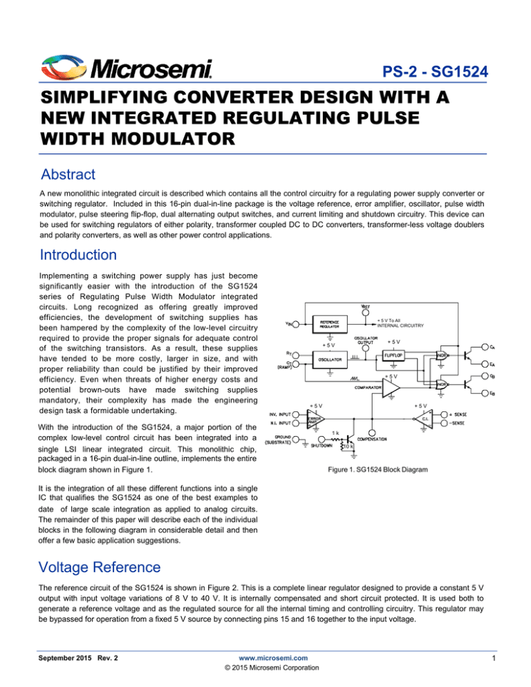
+ 5 V To All
INTERNAL CIRCUITRY
+5V
+5V
+5V
+5V
With the introduction of the SG1524, a major portion of the
complex low-level control circuit has been integrated into a
single LSI linear integrated circuit. This monolithic chip,
packaged in a 16-pin dual-in-line outline, implements the entire
block diagram shown in Figure 1.
+5V
1k
10 k
Figure 1. SG1524 Block Diagram
It is the integration of all these different functions into a single
IC that qualifies the SG1524 as one of the best examples to
date of large scale integration as applied to analog circuits.
The remainder of this paper will describe each of the individual
blocks in the following diagram in considerable detail and then
offer a few basic application suggestions.
Voltage Reference
The reference circuit of the SG1524 is shown in Figure 2. This is a complete linear regulator designed to provide a constant 5 V
output with input voltage variations of 8 V to 40 V. It is internally compensated and short circuit protected. It is used both to
generate a reference voltage and as the regulated source for all the internal timing and controlling circuitry. This regulator may
be bypassed for operation from a fixed 5 V source by connecting pins 15 and 16 together to the input voltage.
September 2015 Rev. 2
www.microsemi.com
© 2015 Microsemi Corporation
1
In this configuration, the maximum input voltage is 6 V.
While discussing input power, it should be mentioned that the
entire SG1524 IC draws less than 10 mA of current, regardless
of input voltage.
This reference may be used as a 5 V source for other circuitry. It
will provide up to 20 mA of output current itself and can easily
be expanded to higher currents with an external PNP transistor
as shown in Figure 3.
1k
1k
25 pF
4k
4.2 k
6.6 V
3. As a convenient place to synchronize an oscilloscope for
system debugging and maintenance.
Figure 2. SG1524 Reference Circuit
4. As a bi-directional port for external timing synchronization.
The output pulse from this oscillator which is stable to
within 2% over variations in both input voltage and temperature - can be used as a master clock for other
circuitry, including other SG1524’s. It thus follows that a
positive pulse applied to this terminal can synchronize the
SG1524 to an external clock signal.
100 Ω
8 V - 40 V
A second output from the oscillator is a narrow clock pulse
which occurs each time CT is discharged. This output pulse is
used for several functions as outlined below:
2. As a trigger for an internal flip-flop which directs the PWM
signal to alternate between the two outputs. Note that for
single-ended applications, the two outputs can be connected in parallel and the frequency of the output is the
frequency of the oscillator. For push-pull applications, the
outputs are separated and the action of the flip-flop provides an output frequency ½ that of the oscillator.
4.2 k
5.9 V
The oscillator in the SG1524 uses an external resistor (RT) to
establish a constant charging current into an external
capacitor(CT). This constant-current charging gives a linear
ramp voltage which provides an overall linear relationship
between error voltage and output pulse width. The SG1524
oscillator circuit is shown in Figure 4.
1. As a blanking pulse to both outputs to insure that there is
no possibility of having both outputs on simultaneously
during transitions. The width of this blanking pulse can be
controlled to some extent by the value selected for CT.
10 k
8.6 k
Oscillator
10 µF
The waveforms of the two outputs from the oscillator are shown
in Figure 5.
Figure 3. SG1524 Expanded Current Source
+5V
7.4 k
20 k
6.2 k
20 k
24 k
1k
3k
Figure 4. SG1524 Oscillator Circuit
Figure 5. SG1524 Oscillator Waveforms
2
Error Amplifier
The error amplifier circuit, shown in Figure 6, is a simple
differential input, transconductance amplifier. Both inputs and
the output are available for maximum versatility. The gain of the
amplifier is nominally 10,000 (80 dB) but can be easily reduced by
either feedback or by shunting the output to ground with an
external resistor. The overall frequency response of this amplifier which, by the way, is not internally compensated but yet is
stable with unity gain feedback, is plotted with various values of
external load resistance in Figure 7.
Phase shifting to compensate for an output filter pole may readily
be accomplished with an external series R-C combination at the
output terminal of the amplifier.
Since the error amplifier is powered by the 5 V reference
voltage, the acceptable common-mode input voltage range is
restricted to 1.8 V to 3.4 V. This means the reference must be
divided down to be compatible with the amplifier input, but yet
provides the advantage of being able to be used to regulate
negative output voltages. Required input dividers are shown in
Figure 8.
5k
5k
5k
5k
Figure 8. Error Amplifier Connections
200 µA
Since this amplifier is a transconductance design, the output is
a very high impedance (approximately 5 MΩ) and can source or
sink only 100 µA. This makes the output terminal (Pin 9) a very
convenient place to insert any programming signal which is to
override the error amplifier. Internal shutdown and current limit
circuits are connected here, but any other circuit which can sink
100 µA can pull this point to ground, thereby shutting off
both outputs.
100 µA
Figure 6. SG1524 Error Amplifier Schematic
For example, the soft start circuit of Figure 9 can be used to hold
Pin 9 to ground - and thus both outputs off - when power is first
applied. As the capacitor charges, the output pulse slowly
increases from zero to the point where the feedback loop takes
control. The diode then isolates this turn-on circuit from whatever
frequency stabilizing network might also be connected to Pin 9.
1 MΩ
300 kΩ
100 kΩ
10
100
1k
10 k
100 k
1M
10 M
Figure 7. SG1524 Error Amp Frequency Response
Figure 9. SG1524 Soft Start Circuitry
3
Current Limiting
The current limiting circuit, while shown in the block diagram as
op-amp, is really only a single transistor amplifier as shown in
Figure 10. It is frequency compensated and has a second
transistor to provide temperature compensation and a reduction
of input threshold to 200 mV. When this threshold is exceeded,
the amplifying transistor turns on and, by pulling the output of the
error amplifier toward ground, linearly decreases the output
pulse width.
5V
10 k
5.1 k
6.2 k
3k
10 k
1k
10 k
10 k
2k
110 µA
Figure 12. SG1524 Over Voltage Protection
25 pF
1k
10 k
1.8 k
Output Stages
The outputs of the SG1524 are two identical NPN transistors with
both collectors and emitters uncommitted. These circuits are as
shown in Figure 13 and include an anti-saturation network for
fast response and current limiting set for an output
current of approximately 100 mA.
10 k
Figure 10. SG1524 Current Limiting
One consideration in using this circuit is that the sense terminals
have a ± 0.3 V common mode range which requires sensing in
the ground line. However, since differential inputs are available,
foldback current limiting can be implemented as shown in
Figure 11.
300 µA
1k
6Ω
Figure 13. SG1524 Output Stage
The availability of both collectors and emitters allows a maximum
versatility to enable driving either NPN or PNP external transistors; however, it must be remembered that this is only a switch
which closes and opens. Power transistor turn-off drive must be
developed externally. Some suggestions for output drive circuits
are shown in Figure 14.
Figure 11. Foldback Current Limiting
While on the subject of protection circuitry, although overvoltage
protection is not built into the SG1524, it is relatively easy to add
by using the internal shutdown circuit in conjunction with a few
external components as shown in Figure 12.
This circuit will provide a low level sensing and latching function
and while it won’t protect against a shorted output transistor, it will
remove the drive signals with no power dissipation.
4
Applications
In considering applications for the SG1524, it appears that there
are three general classifications of switching power supply
systems. Included in the first are the transformerless voltage
multiplier circuits shown in Figure 15. These circuits are primarily
used for low level applications but can step up, step down, or
change the polarity of an input voltage. The switches shown can
be either the output stages of the SG1524 or external transistors.
Note that one extra diode is required to protect the emitter-base
junction of switch SA during the times when both switches are
open.
Figure 16. Single-Ended Inductor Circuits
The third general classification of power supply systems are
transformer coupled, two types of which are shown in Figure 17.
The push-pull circuit represents the conventional DC to DC
converter with each switch being controlled for 0-45% duty
cycle modulation. The second transformer circuit is a singleended flyback converter, useful at light loads without a separate
output inductor.
Figure 14. Driving External Transistors
To illustrate the use of the SG1524 in each of the above general
classifications, the following simple, but practical, circuits are
presented:
Figure 15. Capacitor/Diode Output Circuits
For higher current applications, the single-ended inductor circuits of Figure 16 represent another classification. Here, the two
outputs of the SG1524 are connected in parallel, but note that
this does not give twice the current as the switches are alternating internally. This does not affect external performance, however, and the SG1524 can be used to provide 0-90% duty cycle
modulation in any of the configurations shown.
Figure 17. Transformer Coupled Circuits
5
Figure 18 shows the use of the SG1524 as a low current polarity
converter providing a regulated -5 V output at currents up to
20 mA from a single positive input voltage. The external components required include the divider resistors to interface the
reference and output voltages with the error amplifier, a resistor/
capacitor to set the operating frequency, and the output diodes
and capacitors. The combination of the built-in current limiting of
the SG1524 output stages and the capacitor coupling of the
output signal provide full protection against short circuits and the
current limit amplifier is more than enough to stabilize the
regulating loop and no additional compensation is required.
+ 15 V
For higher current applications, the single-ended conventional
switching regulator of Figure 20 is shown.
15 k
5k
5k
Since the currents in the secondary of a flyback transformer are
out of phase with the primary current, current limiting is very
difficult to achieve. In this circuit, protection was provided
through the use of a soft-start circuit. If either output is shorted,
the transformer will saturate, providing more current through the
drive transistor. This current is sensed and used to turn on the
2N2222 which resets the soft-start circuit and turn off the drive
signal. If the short remains, the regulator will repetitively try to
start up and reset with a time constant set by the soft-start circuit.
Removing the short will then allow the regulating loop to reestablish control.
+ 28 V
20 µF
5k
-5V
20 mA
3k
5k
0.9 mH
68 Ω
5k
+5V
1A
180 Ω
5k
5k
500 µF
2k
3k
50 µF
50 k
Figure 18. Low Current Polarity Converter
0.1 Ω
Another low-level circuit is the flyback converter shown in Figure 19.
+5V
Figure 20. 1 A, Single-Ended Switching Regulator
In this case, an external PNP Darlington is used to provide a
1 A current switch. The SG1524 has the two outputs in parallel,
connected as a grounded emitter amplifier. The current sense
resistor is inserted in the ground line and the voltage across it
used for constant current limiting. Note that in addition to the
divider resistors and frequency setting RTCT, a phase compensation resistor and capacitor is used to stabilize the loop now that
an inductor has been added.
+15 V
25 k
5k
1M
5k
15 V
5k
2k
A fourth application would have to be a push-pull, DC to DC
regulating converter as shown in Figure 21.
1Ω
+ 28 V
Figure 19. +5 V to ±15 V, Flyback Converter
5k
The circuit is designed to develop a regulated ±15 V supply
from a single +5 V source. Note that the reference terminal is
tied to the input, disabling the internal regulator. The error
amplifier resistors are also tied to the input line so that the output
regulation can be no better than the input; however, an external
reference could just as easily have been used.
5k
1k 1k
1W 1W
1 mH
5k
1k
5k
1500 µF
1k
2k
100 µF
20 k
In this application, the two output stages are connected in parallel
and used as emitter followers to drive a single external transistor.
Figure 21. 5 V, 25 W, DC to DC Converter
6
Here the outputs of the SG1524 are connected as separate
emitter followers driving external transistors. Current limiting in
this application is done in the primary for several reasons: First,
it’s easier to live within the ±0.3 V common mode limits of the
current limit amplifier; second, since this is a step-down application, the current - and therefore the power in the sense resistor
- is lower; and third, if the output drive were to become nonsymmetrical causing the transformer to approach saturation, the
resultant current spikes will shorten the pulse width on a
pulse-by-pulse basis, providing a first order correction. Note
that the oscillator is set to run at 40 kHz to obtain a 20 kHz
signal at the transformer.
The application as shown does not provide input-output isolation
and, of course, that feature is difficult to achieve within a single
IC. There are a couple of ways the SG1524 can be used with
isolated power supply systems, however. The first is shown in
Figure 22 where the SG1524 is direct coupled on the secondary
side of the output transformer. The outputs from the IC are
transformer-coupled back to the primary side to drive the switching transistors. Of course, a separate start-up power source is
needed for the SG1524 but that shouldn’t present much of a
problem remembering that the IC draws less than 10 mA
of supply current.
Figure 22. Input/Output Isolation
7
A different method of providing isolation is shown in Figure 23
where the IC is direct coupled on the primary side. Here a
separate reference error amplifier (most easily implemented with
a SG1532 regulator IC) is connected on the secondary and then
optically coupled back to the primary side.
Figure 23. Input/Output Isolation
As should be evident from the above, the SG1524 was designed
as the first of what will undoubtedly become a larger family of
regulator IC’s specifically designed for switching power supplies.
As such, versatility was the primary design goal of this device and
hopefully this goal has been achieved to the degree that will allow
the SG1524 to find application to a wide range of power control
systems.
Microsemi Corporation (Nasdaq: MSCC) offers a comprehensive portfolio of semiconductor and
system solutions for communications, defense & security, aerospace and industrial markets.
Products include high-performance and radiation-hardened analog mixed-signal integrated
circuits, FPGAs, SoCs and ASICs; power management products; timing and synchronization
devices and precise time solutions, setting the world's standard for time; voice processing
devices; RF solutions; discrete components; security technologies and scalable anti-tamper
products; Ethernet solutions; Power-over-Ethernet ICs and midspans; as well as custom
design capabilities and services. Microsemi is headquartered in Aliso Viejo, Calif., and has
approximately 3,600 employees globally. Learn more at www.microsemi.com.
Microsemi Corporate Headquarters
One Enterprise, Aliso Viejo,
CA 92656 USA
Within the USA: +1 (800) 713-4113
Outside the USA: +1 (949) 380-6100
Sales: +1 (949) 380-6136
Fax: +1 (949) 215-4996
E-mail: sales.support@microsemi.com
© 2015 Microsemi Corporation. All
rights reserved. Microsemi and the
Microsemi logo are trademarks of
Microsemi Corporation. All other
trademarks and service marks are the
property of their respective owners.
Microsemi makes no warranty, representation, or guarantee regarding the information contained herein or
the suitability of its products and services for any particular purpose, nor does Microsemi assume any
liability whatsoever arising out of the application or use of any product or circuit. The products sold
hereunder and any other products sold by Microsemi have been subject to limited testing and should not
be used in conjunction with mission-critical equipment or applications. Any performance specifications are
believed to be reliable but are not verified, and Buyer must conduct and complete all performance and
other testing of the products, alone and together with, or installed in, any end-products. Buyer shall not rely
on any data and performance specifications or parameters provided by Microsemi. It is the Buyer's
responsibility to independently determine suitability of any products and to test and verify the same. The
information provided by Microsemi hereunder is provided "as is, where is" and with all faults, and the entire
risk associated with such information is entirely with the Buyer. Microsemi does not grant, explicitly or
implicitly, to any party any patent rights, licenses, or any other IP rights, whether with regard to such
information itself or anything described by such information. Information provided in this document is
proprietary to Microsemi, and Microsemi reserves the right to make any changes to the information in this
document or to any products and services at any time without notice.
PS-2-SG1524 -02/09.15


