10-Bit, 20/40/65/80 MSPS, 1.8V
Dual Analog-to-Digital Converter
AD9204
Preliminary Technical Data
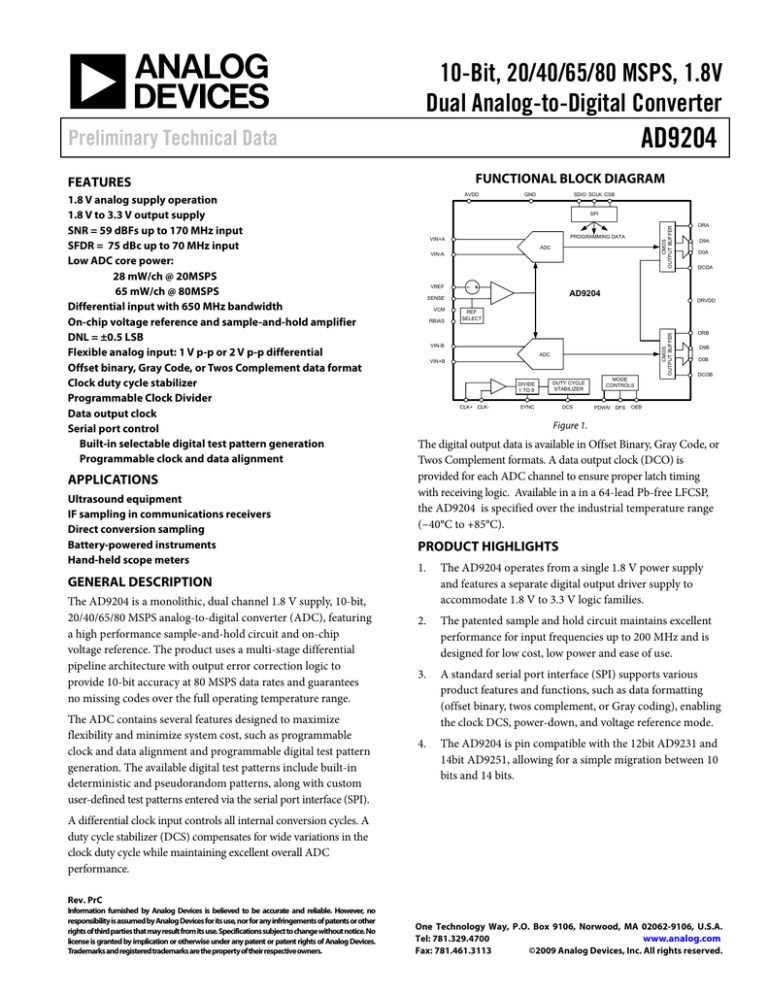
FUNCTIONAL BLOCK DIAGRAM
FEATURES
APPLICATIONS
Ultrasound equipment
IF sampling in communications receivers
Direct conversion sampling
Battery-powered instruments
Hand-held scope meters
The ADC contains several features designed to maximize
flexibility and minimize system cost, such as programmable
clock and data alignment and programmable digital test pattern
generation. The available digital test patterns include built-in
deterministic and pseudorandom patterns, along with custom
user-defined test patterns entered via the serial port interface (SPI).
SDIO SCLK CSB
CMOS
OUTPUT BUFFER
SPI
PROGRAMMING DATA
VIN+A
ADC
VIN-A
ORA
D9A
D0A
DCOA
VREF
AD9204
SENSE
VCM
RBIAS
DRVDD
REF
SELECT
VIN-B
ADC
VIN+B
CLK+ CLK-
DIVIDE
1 TO 8
DUTY CYCLE
STABILIZER
SYNC
DCS
MODE
CONTROLS
PDWN
DFS
ORB
D9B
D0B
DCOB
OEB
Figure 1.
The digital output data is available in Offset Binary, Gray Code, or
Twos Complement formats. A data output clock (DCO) is
provided for each ADC channel to ensure proper latch timing
with receiving logic. Available in a in a 64-lead Pb-free LFCSP,
the AD9204 is specified over the industrial temperature range
(−40°C to +85°C).
PRODUCT HIGHLIGHTS
1.
The AD9204 operates from a single 1.8 V power supply
and features a separate digital output driver supply to
accommodate 1.8 V to 3.3 V logic families.
2.
The patented sample and hold circuit maintains excellent
performance for input frequencies up to 200 MHz and is
designed for low cost, low power and ease of use.
3.
A standard serial port interface (SPI) supports various
product features and functions, such as data formatting
(offset binary, twos complement, or Gray coding), enabling
the clock DCS, power-down, and voltage reference mode.
4.
The AD9204 is pin compatible with the 12bit AD9231 and
14bit AD9251, allowing for a simple migration between 10
bits and 14 bits.
GENERAL DESCRIPTION
The AD9204 is a monolithic, dual channel 1.8 V supply, 10-bit,
20/40/65/80 MSPS analog-to-digital converter (ADC), featuring
a high performance sample-and-hold circuit and on-chip
voltage reference. The product uses a multi-stage differential
pipeline architecture with output error correction logic to
provide 10-bit accuracy at 80 MSPS data rates and guarantees
no missing codes over the full operating temperature range.
GND
CMOS
OUTPUT BUFFER
1.8 V analog supply operation
1.8 V to 3.3 V output supply
SNR = 59 dBFs up to 170 MHz input
SFDR = 75 dBc up to 70 MHz input
Low ADC core power:
28 mW/ch @ 20MSPS
65 mW/ch @ 80MSPS
Differential input with 650 MHz bandwidth
On-chip voltage reference and sample-and-hold amplifier
DNL = ±0.5 LSB
Flexible analog input: 1 V p-p or 2 V p-p differential
Offset binary, Gray Code, or Twos Complement data format
Clock duty cycle stabilizer
Programmable Clock Divider
Data output clock
Serial port control
Built-in selectable digital test pattern generation
Programmable clock and data alignment
AVDD
A differential clock input controls all internal conversion cycles. A
duty cycle stabilizer (DCS) compensates for wide variations in the
clock duty cycle while maintaining excellent overall ADC
performance.
Rev. PrC
Information furnished by Analog Devices is believed to be accurate and reliable. However, no
responsibility is assumed by Analog Devices for its use, nor for any infringements of patents or other
rights of third parties that may result from its use. Specifications subject to change without notice. No
license is granted by implication or otherwise under any patent or patent rights of Analog Devices.
Trademarks and registered trademarks are the property of their respective owners.
One Technology Way, P.O. Box 9106, Norwood, MA 02062-9106, U.S.A.
Tel: 781.329.4700
www.analog.com
Fax: 781.461.3113
©2009 Analog Devices, Inc. All rights reserved.
AD9204
Preliminary Technical Data
64
63
62
61
60
59
58
57
56
55
54
53
52
51
50
49
CLK+
1
48
PDWN
CLK-
2
47
OEB
SYNC
3
46
CSB
NC
4
45
SCLK/DFS
NC
5
44
SDIO/DCS
NC
6
43
ORA
NC
7
42
D9A (MSB)
NC
8
41
D8A
NC
9
40
D7A
39
D6A
D0B (LSB) 11
38
D5A
D1B 12
37
DRVDD
D2B 13
36
D4A
D3B 14
35
D3A
D4B 15
34
D2A
D5B 16
33
D1A
Top View
(not to scale)
DRVDD 10
17
18
19
20
21
22
23
24
25
26
Figure 2. Device Pin Map
Rev. PrC | Page 2 of 4
27
28
29
30
31
32
Preliminary Technical Data
AD9204
Pin #
0
49, 50, 53, 54,
59, 60, 63, 64
10, 19, 28, 37
51, 52
62, 61
1, 2
58
57
56
55
46
45
Name
GND
AVDD
Description
Exposed paddle is the only ground connection for the chip. Must be connected to PCB AGND.
1.8V Analog supply pins.
DRVDD
AINA+/AINB+/CLK+, CLKRBIAS
VCM
SENSE
VREF
CSB
SCLK/DFS
44
SDIO/DCS
Digital Output Driver Supply (1.8V to 3.3V)
Channel “A” analog inputs.
Channel “B” analog inputs.
Differential encode clock; PECL, LVDS or 1.8V CMOS inputs.
Sets analog current bias. Connect to 10kohm (1% tolerance) resistor to ground.
Analog output voltage at mid supply to set common mode of the analog inputs.
Reference Mode Selection
Voltage Reference Input/Output
SPI chip select; active low enable. 50Kohm internal pullup.
SPI clock. Static control of data output format, DFS, if not in SPI mode.
If “high”: twos complement.
If “low”: offset binary.
50Kohm internal pulldown.
SPI data in/out. Static enable for Duty Cycle Stabilizer if not in SPI mode. 50Kohm internal pulldown in
SPI mode. 50Kohm internal pullup in non-SPI mode.
3
47
SYNC
OEB
Digital input. SYNC input to clock divider. 50Kohm internal pulldown.
Digital input. Enable channel “A” & “B” digital outputs if “low”; tri-state outputs if “high”. 50Kohm
internal pulldown.
PDWN
D0B-D9B
D0A-D9A
ORB
ORA
DCOB
DCOA
DNC
Digital input. Powerdown chip if “high”. 50Kohm internal pulldown.
Channel B digital outputs. D9B = MSB
Channel A digital outputs. D9A = MSB
Channel B Out-of-Range digital output.
Channel A Out-of-Range digital output.
Channel B Data Clock digital output.
Channel A Data Clock digital output.
Do Not Connect
48
11-18, 20, 21
32-36, 38-42
22
43
23
24
4-9, 25-27, 29-31
Rev. PrC | Page 3 of 4
AD9204
Preliminary Technical Data
OUTLINE DIMENSIONS
0.60 MAX
9.00
BSC SQ
0.60
MAX
64
49
48
PIN 1
INDICATOR
1
PIN 1
INDICATOR
8.75
BSC SQ
0.50
BSC
0.50
0.40
0.30
1.00
0.85
0.80
SEATING
PLANE
33
32
16
17
0.25 MIN
7.50
REF
0.80 MAX
0.65 TYP
12° MAX
0.05 MAX
0.02 NOM
0.30
0.23
0.18
6.35
6.20 SQ
6.05
EXPOSED PAD
(BOTTOM VIEW)
0.20 REF
FOR PROPER CONNECTION OF
THE EXPOSED PAD, REFER TO
THE PIN CONFIGURATION AND
FUNCTION DESCRIPTIONS
SECTION OF THIS DATA SHEET.
COMPLIANT TO JEDEC STANDARDS MO-220-VMMD-4
091707-C
TOP VIEW
Figure 3. 64-Lead Lead Frame Chip Scale Package [LFCSP_VQ]
9 mm × 9 mm Body, Very Thin Quad (CP-64-4)
Dimensions shown in millimeters
ORDERING GUIDE
Model
AD9204BCPZ-801 2
AD9204BCPZRL7–801,2
AD9204BCPZ-651,2
AD9204BCPZRL7–651,2
AD9204BCPZ-401,2
AD9204BCPZRL7–401,2
AD9204BCPZ-201,2
AD9204BCPZRL7–201,2
AD9204Z-80EB1
AD9204Z-65EB1
AD9204Z-40EB1
AD9204Z-20EB1
1
2
Temperature Range
–40°C to +85°C
–40°C to +85°C
–40°C to +85°C
–40°C to +85°C
–40°C to +85°C
–40°C to +85°C
–40°C to +85°C
–40°C to +85°C
Package Description
64-Lead Lead Frame Chip Scale Package (LFCSP_VQ)
64-Lead Lead Frame Chip Scale Package (LFCSP_VQ)
64-Lead Lead Frame Chip Scale Package (LFCSP_VQ)
64-Lead Lead Frame Chip Scale Package (LFCSP_VQ)
64-Lead Lead Frame Chip Scale Package (LFCSP_VQ)
64-Lead Lead Frame Chip Scale Package (LFCSP_VQ)
64-Lead Lead Frame Chip Scale Package (LFCSP_VQ)
64-Lead Lead Frame Chip Scale Package (LFCSP_VQ)
Evaluation Board
Evaluation Board
Evaluation Board
Evaluation Board
Z = Pb-free part.
The exposed paddle is the only GND connection on the chip and must be connected to the PCB AGND.
©2009 Analog Devices, Inc. All rights reserved. Trademarks and
registered trademarks are the property of their respective owners.
PR08122-0-4/09(PrC)
Rev. PrC | Page 4 of 4
Package Option
CP-64-4
CP-64-4
CP-64-4
CP-64-4
CP-64-4
CP-64-4
CP-64-4
CP-64-4
