NCV7718GEVB Test Procedure
advertisement

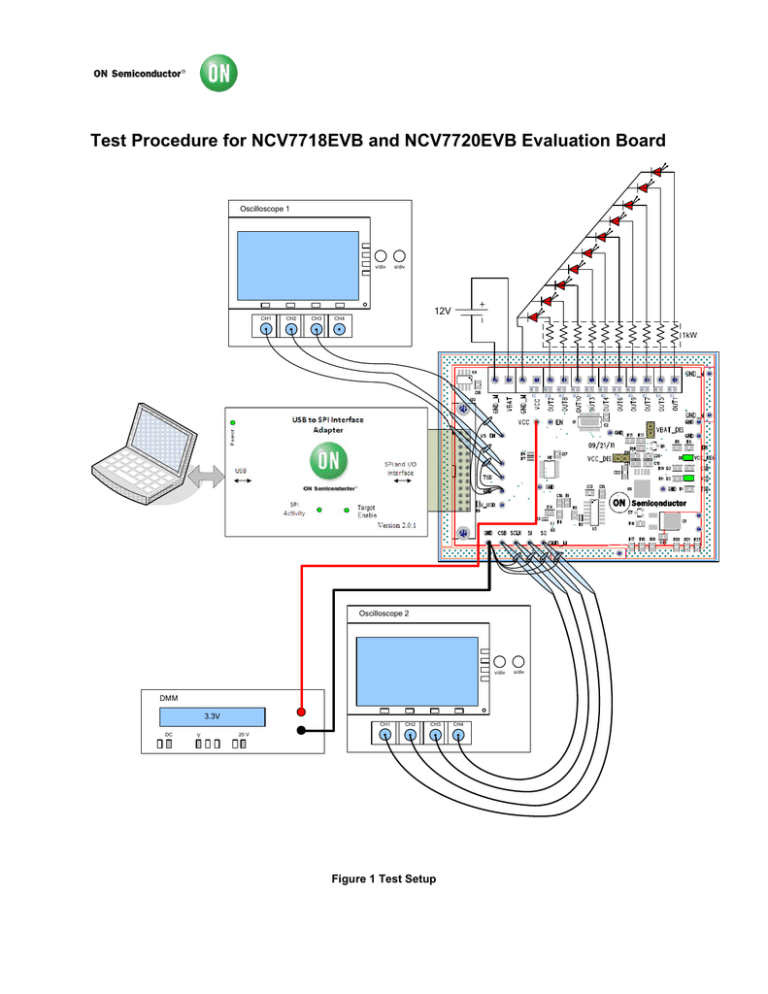
Test Procedure for NCV7718EVB and NCV7720EVB Evaluation Board Oscilloscope 1 v/div CH1 CH2 CH3 s/div 12V CH4 1kW Oscilloscope 2 v/div DMM 3.3V CH1 DC V CH2 CH3 20 V Figure 1 Test Setup CH4 s/div As shown in the test setup, the jumper VCC_DIS and VBAT_DIS should be populated. Equipment: The required equipment to test the NCV7718 and the NCV7720 evaluation board is listed hereunder: Equipment Oscilloscope DC Power Supply Resistive Load LEDs PC with FlexMOS GUI installed USB to SPI interface Adapter USB Type A to Type B cable 24 Pin Ribbon Cable Quantity 2 1 6 for NCV7718, 10 for NCV7720 6 for NCV7718, 10 for NCV7720 1 1 Basic Specifications Quad Channel Oscilloscope 6V - 40V, 2A 1 kΩ <75 mA Windows XP or higher Version 2.0.1 or higher 1 - 1 - The LEDS provide visual indication of the outputs turning on and off. The output loads could be purely resistive and output transition can be monitored via an oscilloscope. Test Procedure: 1. Visual Check: When 12V is applied to VBAT, the VCC_REG and VCC LEDs should be illuminated. This indicates that the onboard regulators are operational. Check the VCC voltage on DMM to confirm that the regulated VCC voltage is 3.3V. 2. Programmed EEPROM When the FlexMOS GUI is launched, the dedicated GUI for the evaluation should be automatically selected from the drop down list. If the device name is not recognized the onboard EEPROM needs to be programmed. The EEPROM must be programmed when the target board (NCV7718GEVB or NCV7720GEVB) is attached. 3. VCC 5V Operation: The onboard regulator can be programmed for 5V operation. Select the 5V radio button on the VCC mode box. Check the DMM to see if the VCC is now being regulated to 5V. If 5V radio button does not update DMM to 5V, connect secondary DC source to the V5_EN pin, and apply 5V. 4. Enabling the Device: Click the Enable Check Box on the bottom of the GUI and confirm that the EN LED is illuminated at this time. The orange “Target” LED on SPI will also be lit. 5. Turn On/Off Outputs in High Side Configuration The load configuration shown in Figure 1 is an example of the half-bridge driver configured in high side topology. One by one turn on the high side drivers (HS ON) to insure the proper driver functionality. If any of the drivers failed to turn on, check for any faults on the SO diagnostics and the transmitted SPI frame with an oscilloscope to ensure that the correct bits were sent to the device. The ALL OFF push button could be used to turn the drivers off. 6. TSD Behavior The TSD behavior can be verified by sending a frame with B0 (OVLO – Over Voltage) set high and then pressing the TSD push button. This should illuminate the TSD LED since SI is OR’ed with the TSD bit (SI holds the value of B0 until the next rising edge of SCLK on the next SPI cycle). Hit update twice to turn TSD LED on/off. Or hit update once and click the TSD button to turn TSD LED on/off.


