View PDF - OMICS International
advertisement
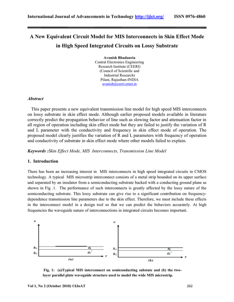
International Journal of Advancements in Technology http://ijict.org/ ISSN 0976-4860 A New Equivalent Circuit Model for MIS Interconnects in Skin Effect Mode in High Speed Integrated Circuits on Lossy Substrate Avanish Bhadauria Central Electronics Engineering Research Institute (CEERI) (Council of Scientific and Industrial Research) Pilani, Rajasthan-INDIA avanish@ceeri.ernet.in Abstract This paper presents a new equivalent transmission line model for high speed MIS interconnects on lossy substrate in skin effect mode. Although earlier proposed models available in literature correctly predict the propagation behavior of line such as slowing factor and attenuation factor in all region of operation including skin effect mode but they are failed to justify the variation of R and L parameter with the conductivity and frequency in skin effect mode of operation. The proposed model clearly justifies the variation of R and L parameters with frequency of operation and conductivity of substrate in skin effect mode where other models failed to explain. Keywords :Skin Effect Mode, MIS Interconnects, Transmission Line Model 1. Introduction There has been an increasing interest in MIS interconnects in high speed integrated circuits in CMOS technology. A typical MIS microstrip interconnect consists of a metal strip bounded on its upper surface and separated by an insulator from a semiconducting substrate backed with a conducting ground plane as shown in Fig .1. The performance of such interconnects is greatly affected by the lossy nature of the semiconducting substrate. This lossy substrate can give rise to a significant contribution on frequencydependence transmission line parameters due to the skin effect. Therefore, we must include these effects in the interconnect model in a design tool so that we can predict the behaviors accurately. At high frequencies the waveguide nature of interconnections in integrated circuits becomes important. Fig. 1: (a)Typical MIS interconnect on semiconducting substate and (b) the twolayer parallel plate waveguide structure used to model the wide MIS microstrip. Vol 1, No 2 (October 2010) ©IJoAT 262 International Journal of Advancements in Technology http://ijict.org/ ISSN 0976-4860 The MIS interconnects on lossy substrate have been widely studied by Guckel et al. [1], Hasegawa et al. [2], and Jaeger [3] and they proposed their own equivalent circuit models. Guckel et al. first observed that when the substrate conductivity is greater than a specific conductivity, the MIS line is dominated by series loss, and that when is less then , the MIS line will be dominated by shunt loss. They treated these two regions of operation independently and developed different equivalent-circuit descriptions for each of them. Hasegawa et al. have further extended these concepts in [2]. He proposed three different regions of operation namely lossy dielectric region, slow wave region and skin effect region and proposed its own distinct equivalent-circuit model. Jaeger [3] primarily studied the “slow wave” region of propagation. He proposed quite differently from the treatments of [1] and [2] by proposing an equivalentcircuit model in which the resistance of the lossy substrate is connected in parallel with the resistances of the metal and insulator, rather than in series with them. Brews [4] and Williams [5] have also presented their equivalent models using different approaches. Further, we have also proposed a highly accurate unified transmission line model [6] using modal field solution. We have extensively studied the skin effect mode. But none of these models were capable to explain and justify the inductance and resistance parameter variation with the conductivity and frequency in skin effect mode of operation. In this paper we have proposed a new circuit configuration with new circuit elements which explains the variation of R and L parameters with conductivity and frequency as described in earlier models. Most of the transmission line model reported in literature[1]-[7] consist of series impedance Z, i.e., the series combination of resistance R and inductance L with shunt admittance Y, i.e., the combination of conductance G and capacitance C as represented in Fig 2 (a). The Shunt admittance part can further be separated as a series combination of capacitor C1 due to insulator and lossy capacitor C2* due to semiconducting substrate as shown in Fig 2(b). The capacitance due to lossy substrate can accurately be represented by parallel combination of resistor with conductance G and capacitance C2. This circuit representation of shunt admittance correctly predicts the circuit behavior of line under the influence of the conductivity and also predicts the propagation behavior correctly in lossy dielectric region of operation. Further, the expanded representation of series impedance part of transmission line model [1]-[6] as has been shown in Fig 2b, consists of inductance L1 due to insulating layer, Inductance L2 due to substrate layer and resistance R due to loss in semiconductor. However, the model for skin effect described by this series combination correctly predicts the propagation behavior such as slowing factor and attenuation but not able to justify the behavior of circuit elements with the variation of conductivity in semiconducting substrate and frequency of operation. 2. Field Analysis of MIS structure A broad MIS interconnect can be well approximated to a two-layer parallel plate waveguide structure with layers of dielectric constants 1 and 2* shown in Fig 1. The dielectric constant of second layer is complex and is obtained by expression [6]. Vol 1, No 2 (October 2010) ©IJoAT 263 International Journal of Advancements in Technology http://ijict.org/ ISSN 0976-4860 The magnetic field Hy(x) of the TM fields in this planar waveguide satisfies the equation d 2H y dx 2 (1) k 0 ( *i ( x) *2 / k 0 2 ) H y 0 and Hy(x) for the TM modes is obtained by solving above wave equation with appropriate boundary conditions: H ( y ) H 0 cos(1x) H0 0 x h1 (2) cos(1h1 ) cos[ 2 ( x h)] h1 x h cos( 2 h2 ) where, m (k 02 m *2 )1 / 2 , k 0 2 / 0 is the free space propagation constant, * j is the complex propagation constant. / k 0 , also referred to as the slowing factor and is the attenuation constant. We carried out calculations for a typical MIS line on a silicon substrate of thickness h2 = 190m with an insulating (SiO2) layer of thickness h1=0.3m and dielectric constant 1=4.5. 3. Equivalent Inductance in Skin Effect Mode The complex series inductance due to skin effect can be written as the ratio of the magnetic flux linkage to the current as L* 1 B.ds I (3) Where, I, the total current in the strip conductor of width W can be obtained from the line integral of H y around the conductor at the surface as I H .dl H 0W . While the flux linkage for length z is obtained as B.ds h (4) 0 z H y .dx 0 Substituting Hy from the above field solution Eq.(2) and hence the complex inductance L* per unit length for unit width can be obtained as, (5) L* L jL 0 h1' h2' where, sin(1h1 ) h1' h1 1h1 Vol 1, No 2 (October 2010) ©IJoAT and h2' h2 sin( 2 h2 ) . 2 h2 264 International Journal of Advancements in Technology http://ijict.org/ ISSN 0976-4860 The real part of the complex inductance L* corresponds to a series inductance L , while the imaginary part defines the series resistance, R( ) L . 4. New Equivalent Model The model shown in Fig 3 for skin effect described by a series combination of these inductances and resistance are not really circuit element they are just the real and imaginary part of series impedance obtained from parameter extraction. Therefore, they are further need to be expanded to study the correct behavior of circuit elements with conductivity and frequency. In earlier models the series impedance circuit elements, L1, L2 and R, all are in series combination. The series combination of resistance R with inductance L2 due to substrate layer is not capable to explain the variation of and inductance at very high and low conductivities and frequencies. As per earlier models [5]-[6], when conductivity of the substrate becomes very low and goes to zero the resistance of the substrate should be infinite and hence line will be open circuited as the resistance is in series and signal should not propagate which is practically impossible. Further if conductivity in substrate is very high, i.e., infinite, then as per old model total inductance will be L1,+ L2 , which is also impossible as per plot of inductance at low conductivity predicted in the plot by old model. This is also not possible theoretically and is only possible, when substrate is pure insulator as opposed to case. Hence the existing model needs to be corrected. Similarly the variation of equivalent resistance with conductivity is also not justified. Fig. 3: New equivalent of transmission line model of MIS line As the resistance corresponds to a leakage current due to longitudinal electric field Ez, caused by the tangential magnetic field Hy as in Eq.(2) which directly contributes the inductance of the lossy substrate in the structure. These fields are in parallel in direction and hence the circuit Vol 1, No 2 (October 2010) ©IJoAT 265 International Journal of Advancements in Technology http://ijict.org/ ISSN 0976-4860 elements R and L would have to be parallel in combination rather than in series as presented in literature. Hence, we propose a new modification in the model by introducing a resistance with the inductance in parallel rather than in series. This resistance is a structural resistance of substrate and the inductance is nothing but the structural inductance of the substrate in case of the zero conductivity. Structural Inductance of the MIS structure in absence of conductivity L 0 h1 h2 W (6) L 0 h1 0 h2 L1 L2 W W (7) L1 and L2 are the inductance of insulating layer and semiconductor layer with zero conductivity. The total inductance is sum of individual inductance of each layer. And the structural resistance of semiconductor is simply given by R 1 W h1 h2 (8) The behavior of each circuit parameters, i.e., series inductance and series resistance as obtained by earlier model can be reproduced by this new model by calculating the series impedance as Z1 z1 z 2 jR1L1 jL1 R1 jL2 L* L1 L' L1 (9) RL2 jRL2 j 2 2 2 2 R L R 2 L2 2 2 R' L2 2 L22 L 1 R2 (10) (11) R / 2 1 R / L2 While L’ and R’ are the conventional series inductance and resistance. This equivalent model correctly justifies the following cases very honestly: Lim R 0 L' L1 , Lim R L' L1 L2 Lim R 0 R ' 0 , Lim R R ' 0 Lim 0 L' L1 L2 , Lim 0 L' L1 Vol 1, No 2 (October 2010) ©IJoAT 266 International Journal of Advancements in Technology http://ijict.org/ ISSN 0976-4860 Lim R ' 0 , Lim o R ' 0 5. Results and Discussion Results for circuit parameters R and L have been obtained by new model and earlier approaches are shown in Fig 4 and Fig 5.These parameters for a MIS line are defined per unit length per unit width. The new circuit elements and configuration of new model clearly justificatory the behavior of R and L parameters in earlier model. Results obtained from model reveals that the structural dimensions play a very important role in skin effect behavior. It has also been observed that definition of complex Inductance used in earlier model only gives the relationship between flux and current and voltage which finally gives more precisely the impedance rather than individual circuit elements. 6. Conclusion We have presented a new equivalent circuit model for MIS interconnects in skin effect mode of operation in high speed circuits on lossy substrate. The model explains the dependence of inductance and resistance on conductivity and frequency of operation in lossy substrate predicted by earlier model. This new model also has good agreement with the earlier model. This model is more realistic then the earlier one as it explains the limiting condition such as at very high frequency and very high conductivity. The newly extracted Circuit parameters found to be frequency independent and more generalized in nature. It also justifies the frequency dependence of R and L parameters in skin effect as appears in earlier models. Although this model correctly explains the high frequency behavior in skin effect mode in the MIS line but there is a need to improve the accuracy for the results. Hence we need to develop a methodology for parameter extraction from the field solutions also. Vol 1, No 2 (October 2010) ©IJoAT 267 International Journal of Advancements in Technology http://ijict.org/ 0.3 2.50E-10 0.25 Inductance (H) Inductance (nH) 0.5GHz 0.5GHz 0.2 1.0GHz 0.15 1.5GHz 0.1 1.50E-10 1.00E-10 1.0GHz 1.5GHz 5.00E-11 0.05 0 1E+21 1E+22 1E+23 1E+24 1E+25 Carrier Concentration(/m3) 1 0.00E+00 1.00E+20 1.00E+21 1.00E+22 1.00E+23 1.00E+24 1.00E+25 Carrier Concentration (/m3) Fig 4(a) : Variation of Equivalent inductance L(nH) with different carrier concentrations at different frequencies. Fig 5(a) : Variation of Equivalent inductance L(nH) with different carrier concentrations at different frequencies by new model. 1.00E+00 1.5GHz 0.9 9.00E-01 0.8 8.00E-01 0.7 0.5 0.4 1.5GHz 7.00E-01 1.0GHz 0.6 0.5GHz Resistance(Ohm) Resistance(R) 0.1GHz 2.00E-10 0.1GHz 1E+20 ISSN 0976-4860 0.3 6.00E-01 5.00E-01 4.00E-01 3.00E-01 0.2 1.0GHz 0.5GHz 2.00E-01 0.1 0.1GHz 1.00E-01 0.1GHz 0 1E+20 1E+21 1E+22 1E+23 Carrier Concentration(/m3) 1E+24 1E+25 0.00E+00 1.00E+19 1.00E+20 1.00E+21 1.00E+22 1.00E+23 1.00E+24 1.00E+25 Carrier Concentration (/m3) Figure 4(b) Variation of resistance R(ohm) with carrier concentrations at different frequencies. Vol 1, No 2 (October 2010) ©IJoAT Fig 5(b): Variation of resistance R(ohm) with carrier concentrations at different frequencies obtained by new model 268 International Journal of Advancements in Technology http://ijict.org/ ISSN 0976-4860 References [1] H. Guckel, P. A. Brennan, and I. Pal´ocz, “A parallel-plate waveguide approach to microminiaturized, [2] [3] [4] [5] [6] planar transmission lines for integrated circuits,” IEEE Trans. Microwave Theory Tech., vol. MTT-15, pp. 468–476, Aug. 1967. H. Hasegawa, M. Furukawa, and H. Yanai, “Properties of microstrip line on SiSiO2 system,” IEEE Trans. Microwave Theory Tech., vol. MTT-19, pp. 869–881, Nov. 1971. D. Jaeger, “Slow-wave propagation along variable Schottky-contact microstrip line,” IEEE Trans. Microwave Theory Tech., vol. MTT-24, pp. 566–573, Sept. 1976. D. F. Williams, “Metal–Insulator–Semiconductor Transmission Lines,” IEEE transactions on Microwave Theory and Techniques. vol. 47, pp.176–181, Fab. 1999 Avanish Bhadauria, E. K. Sharma and A. K. Verma, “Equivalent Transmission Line Model for Optically Controlled Miscrostrip Slow Wave Structures,” Microwave and Optical Technology Letters, vol. 31, pp. 292-298, No. 4 (2001). J. R. Brews, “Transmission line models for lossy waveguide interconnections in VLSI,” IEEE Trans. Electron Devices, vol. ED-33, pp.1356–1365, Sept. 1986 Vol 1, No 2 (October 2010) ©IJoAT 269
