DATASHEET
IDT5P50901/2/3/4
SPREAD SPECTRUM CLOCK SYNTHESIZER
Description
Features
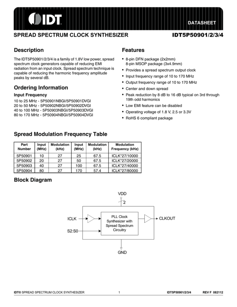
The IDT5P50901/2/3/4 is a family of 1.8V low power, spread
spectrum clock generators capable of reducing EMI
radiation from an input clock. Spread spectrum technique is
capable of reducing the harmonic frequency amplitude
peaks by several dB.
• 8-pin DFN package (2x2mm)
8-pin MSOP package (3x4.9mm)
•
•
•
•
•
Ordering Information
Input Frequency
10 to 25 MHz - 5P50901NBGI/5P50901DVGI
20 to 50 MHz - 5P50902NBGI/5P50902DVGI
40 to 100 MHz - 5P50903NBGI/5P50903DVGI
80 to 170 MHz - 5P50904NBGI/5P50904DVGI
Provides a spread spectrum output clock
Input frequency range of 10 to 170 MHz
Output frequency range of 10 to 170 MHz
Center and down spread
Peak reduction by 8 dB to 16 dB typical on 3rd through
19th odd harmonics
• Low EMI feature can be disabled
• Operating voltage of 1.8 V, 2.5 or 3.3V
• RoHS 6 compliant package
Spread Modulation Frequency Table
Part
Number
Input
(MHz)
Modulation
(kHz)
Input
(MHz)
Modulation
(kHz)
Modulation
Frequency (kHz)
5P50901
5P50902
5P50903
5P50904
10
20
40
80
27
27
27
27
25
50
100
170
67.5
67.5
67.5
57.4
ICLK*27/10000
ICLK*27/20000
ICLK*27/40000
ICLK*27/80000
Block Diagram
VDD
2
ICLK
S2:S0
PLL Clock
Synthesizer with
Spread Spectrum
Circuitry
CLKOUT
GND
IDT® SPREAD SPECTRUM CLOCK SYNTHESIZER
1
IDT5P50901/2/3/4
REV F 082112
IDT5P50901/2/3/4
SPREAD SPECTRUM CLOCK SYNTHESIZER
CLOCK SYNTHESIZER
Pin Assignment
ICLK
1
VDD
8
CLKOUT
VDD
S0
GND
4
S1
5
S2
8-pin DFN
Spread Direction and Percentage Select Table
S2
S1
S0
Spread
Direction
Spread
Percentage
0
0
0
0
1
1
1
1
0
0
1
1
0
0
1
1
0
1
0
1
0
1
0
1
OFF
Center
Center
Center
Center
Center
Down
Down
-±0.25
±0.5
±1.0
±1.5
±2.0
-0.5
-1.0
Pin Description
Pin
Number
Pin
Name
Pin Type
Pin Description
1
ICLK
Input
Input clock.
2
VDD
Power
Voltage supply. Connect to 1.8 V ±0.1 V, 2.5 V ±10% or 3.3 V ±10%,
3
S0
Input
Function select 0 input. Selects spread amount and direction per table above.
Internal pull-down resistor.
4
S1
Input
Function select 1 input. Selects spread amount and direction per table above.
Internal pull-down resistor.
5
S2
Input
Function select 2 input. Selects spread amount and direction per table above.
Internal pull-down resistor.
6
GND
Power
Connect to ground.
7
CLKOUT
Output
Clock output.
8
VDD
Power
Voltage supply. Connect to 1.8 V ±0.1 V, 2.5 V ±10% or 3.3 V ±10%
IDT® SPREAD SPECTRUM CLOCK SYNTHESIZER
2
IDT5P50901/2/3/4
REV F 082112
IDT5P50901/2/3/4
SPREAD SPECTRUM CLOCK SYNTHESIZER
CLOCK SYNTHESIZER
External Components
Decoupling Capacitor
PCB Layout Recommendations
As with any high-performance mixed-signal IC, the
IDT5P50901/2/3/4 must be isolated from system power
supply noise to perform optimally.
For optimum device performance and lowest output phase
noise, the following guidelines should be observed.
1) The 0.01µF decoupling capacitors should be mounted on
the component side of the board as close to the VDD pin as
possible. No vias should be used between the decoupling
capacitors and VDD pins. The PCB trace to VDD pins
should be kept as short as possible, as should the PCB
trace to the ground via.
A decoupling capacitor of 0.01µF must be connected
between each VDD and the PCB ground plane.
Series Termination Resistor
Clock output traces over one inch should use series
termination. To series terminate a 50Ω trace (a commonly
used trace impedance), place a 33Ω resistor in series with
the clock line, as close to the clock output pin as possible.
The nominal impedance of the clock output is 20Ω.
2) To minimize EMI, the 33Ω series termination resistor (if
needed) should be placed close to the clock output.
3) An optimum layout is one with all components on the
same side of the board, minimizing vias through other signal
layers. Other signal traces should be routed away from the
IDT5P50901/2/3/4. This includes signal traces just
underneath the device, or on layers adjacent to the ground
plane layer used by the device.
External Clock Input
This device operates from an external clock input and as
such does not have a on chip oscillator circuit.
Spread Spectrum Profile
The IDT5P50901/2/3/4 is a low EMI clock generator using
an optimized frequency slew rate algorithm to facilitate down
stream tracking of zero delay buffers and other PLL devices.
The modulation rate is directly relate to the input clock
frequency.
For input frequency ICLK, then use the modulation
frequency indicated for the part below.
Frequency
Modulation Rate
Time
IDT® SPREAD SPECTRUM CLOCK SYNTHESIZER
3
IDT5P50901/2/3/4
REV F 082112
IDT5P50901/2/3/4
SPREAD SPECTRUM CLOCK SYNTHESIZER
CLOCK SYNTHESIZER
Absolute Maximum Ratings
Stresses above the ratings listed below can cause permanent damage to the IDT5P50901/2/3/4. These ratings,
which are standard values for IDT commercially rated parts, are stress ratings only. Functional operation of the
device at these or any other conditions above those indicated in the operational sections of the specifications is not
implied. Exposure to absolute maximum rating conditions for extended periods can affect product reliability.
Electrical parameters are guaranteed only over the recommended operating temperature range.
Item
Rating
Supply Voltage, VDD
-0.5 V to 5.0 V
All Inputs
-0.5 V to VDD +0.5 V
Ambient Operating Temperature
-40 to +85° C
Storage Temperature
-50 to +150° C
Junction Temperature
125° C
Soldering Temperature
260° C
Recommended Operation Conditions
Parameter
Min.
Typ.
Max.
Units
+85
°C
Ambient Operating Temperature
-40
Power Supply Voltage VDD (measured in respect to GND)
+1.7
+1.8
+1.9
V
+2.25
+2.5
+2.75
V
+2.97
+3.3
+3.63
V
IDT® SPREAD SPECTRUM CLOCK SYNTHESIZER
4
IDT5P50901/2/3/4
REV F 082112
IDT5P50901/2/3/4
SPREAD SPECTRUM CLOCK SYNTHESIZER
CLOCK SYNTHESIZER
DC Electrical Characteristics
Unless stated otherwise, VDD = 1.8 V ±0.1 V. Ambient Temperature -40 to +85° C
Parameter
Symbol
Conditions
Min.
Typ.
Max.
Units
1.7
1.8
1.9
V
Operating Voltage
VDD
Input High Voltage
VIH
ICLK, S2:S0
VDD x 0.8
VDD + 0.3
V
Input Low Voltage
VIL
ICLK, S2:S0
GND
VDD x 0.2
V
Output High Voltage
VOH
IOH = -12 mA
VDD x 0.75
Output Low Voltage
VOL
IOL = 12 mA
IDD
VDD
GND
No load
V
VDD x 0.25
V
See table page 6
Input Capacitance
5
pF
Load Capacitance
5
pF
Internal Pull-down
Resistor
RPD
S1:S0
200
260
kΩ
Unless stated otherwise, VDD = 2.5 V ±10%. Ambient Temperature -40 to +85° C
Parameter
Symbol
Conditions
Min.
Typ.
Max.
Units
2.25
2.5
2.75
V
Operating Voltage
VDD
Input High Voltage
VIH
ICLK, S2:S0
VDD x 0.8
VDD + 0.3
V
Input Low Voltage
VIL
ICLK, S2:S0
GND
VDD x 0.2
V
Output High Voltage
VOH
IOH = -25 mA
VDD x 0.9
Output Low Voltage
VOL
IOL = 25 mA
IDD
VDD
GND
No load
V
VDD x 0.1
V
See table page 6
Input Capacitance
5
pF
Load Capacitance
5
pF
Internal Pull-down
Resistor
RPD
S1:S0
200
260
kΩ
Unless stated otherwise, VDD = 3.3 V ±10%. Ambient Temperature -40 to +85° C
Parameter
Symbol
Conditions
Min.
Typ.
Max.
Units
2.97
3.3
3.63
V
Operating Voltage
VDD
Input High Voltage
VIH
ICLK, S2:S0
VDD x 0.8
VDD + 0.3
V
Input Low Voltage
VIL
ICLK, S2:S0
GND
VDD x 0.2
V
Output High Voltage
VOH
IOH = -33 mA
VDD x 0.9
Output Low Voltage
VOL
IOL = 33 mA
IDD
VDD
GND
No load
V
VDD x 0.1
V
See table page 6
Input Capacitance
5
pF
Load Capacitance
5
pF
Internal Pull-down
Resistor
RPD
IDT® SPREAD SPECTRUM CLOCK SYNTHESIZER
S1:S0
200
5
260
IDT5P50901/2/3/4
kΩ
REV F 082112
IDT5P50901/2/3/4
SPREAD SPECTRUM CLOCK SYNTHESIZER
CLOCK SYNTHESIZER
Operational IDD
IDT5P50901
IDT5P50902
5.00
7.00
4.50
6.00
4.00
5.00
3.50
Idd (mA)
Idd (mA)
3.00
2.50
2.00
3.3V
1.50
2.5V
4.00
3.00
3.3V
2.00
1.8V
1.00
2.5V
1.00
0.50
0.00
1.8V
0.00
10
15
20
25
20
25
30
Fin
35
40
45
50
Fin (MHz)
IDT5P50904
IDT5P50903
9.00
14.00
8.00
12.00
7.00
10.00
Idd (mA)
Idd (mA)
6.00
5.00
4.00
8.00
6.00
3.3V
3.00
4.00
2.5V
2.00
3.3V
2.5V
1.8V
2.00
1.8V
1.00
0.00
0.00
40
50
60
70
80
90
80
100
100
120
140
160
Fin (MHz)
Fin (MHz)
AC Electrical Characteristics
Unless stated otherwise, VDD = 1.8 V ±0.1 V, 2.5 V ±10% or 3.3 V ±10%. Ambient Temperature -40 to +85° C
Parameter
Symbol
Conditions
Output Clock Duty Cycle
1.8V ±0.1V, >130MHz
Min.
Typ.
Max. Units
45
50
55
40
50
60
%
Output Rise Time
tOR
20% to 80%, Note 1
1.2
ns
Output Fall Time
tOF
80% to 20%, Note 1
1.2
ns
Spread Spectrum Modulation
Rate
10 to 25 MHz input (IDT5P50901)
27
67.5
kHz
20 to 50 MHz input (IDT5P50902)
27
67.5
kHz
40 to 100 MHz input (IDT5P50903)
27
67.5
kHz
80 to 170 MHz input (IDT5P50904)
27
57.3
kHz
Jitter Cycle to Cycle
Cycle to cycle jitter
Output Settling Time
Note 2
150
ps
3.0
ms
Note 1: Measured with 5 pF load
Note 2: Time between VDD rising above minimum operating voltage and stable frequency output
IDT® SPREAD SPECTRUM CLOCK SYNTHESIZER
6
IDT5P50901/2/3/4
REV F 082112
IDT5P50901/2/3/4
SPREAD SPECTRUM CLOCK SYNTHESIZER
CLOCK SYNTHESIZER
Package Outline and Package Dimensions (8-pin DFN 2x2mm, 0.5mm pitch)
Package dimensions are kept current with JEDEC Publication No. 95,
Symbol
A
A1
A3
b
N
ND
NE
D
E
e
D2
E2
L
aaa
bbb
ccc
Min
Millimeters
Max
0.80
1.00
0
0.05
0.20 Reference
0.20
0.30
8
4
0
2.00 BASIC
2.00 BASIC
0.50 BASIC
1.05
1.25
0.45
0.65
0.20
0.40
0.15
0.10
0.10
Marking Diagram (8DFN)
5
8
####
9xGI
4
1
Notes:
1. #### is the last four numbers of the lot number.
2. Dot indicates pin 1.
3. “G” designates Pb (lead) free package.
IDT® SPREAD SPECTRUM CLOCK SYNTHESIZER
7
IDT5P50901/2/3/4
REV F 082112
IDT5P50901/2/3/4
SPREAD SPECTRUM CLOCK SYNTHESIZER
CLOCK SYNTHESIZER
Package Outline and Package Dimensions (8-pin MSOP, 3.00 mm Body)
Package dimensions are kept current with JEDEC Publication No. 95
Millimeters
8
Symbol
E1
A
A1
A2
b
C
D
E
E1
e
L
α
aaa
E
IN D E X
AREA
1
2
D
Min
Max
-1.10
0
0.15
0.79
0.97
0.22
0.38
0.08
0.23
3.00 BASIC
4.90 BASIC
3.00 BASIC
0.65 Basic
0.40
0.80
0°
8°
0.10
Inches*
Min
Max
-0.043
0
0.006
0.031
0.038
0.008
0.015
0.003
0.009
0.118 BASIC
0.193 BASIC
0.118 BASIC
0.0256 Basic
0.016
0.032
0°
8°
0.004
*For reference only. Controlling dimensions in mm.
A
2
A
A
1
c
-C e
b
S E A T IN G
P LA N E
L
aaa
C
Marking Diagram (8 MSOP)
5
8
YYWW
90xGI
4
1
Notes:
1.YYWW is the assembly date code.
2. Dot indicates pin 1.
3. “G” designates Pb (lead) free package.
4. “I” designates industrial temperature range.
IDT® SPREAD SPECTRUM CLOCK SYNTHESIZER
8
IDT5P50901/2/3/4
REV F 082112
IDT5P50901/2/3/4
SPREAD SPECTRUM CLOCK SYNTHESIZER
CLOCK SYNTHESIZER
Ordering Information
Part / Order Number
5P50901NBGI8
5P50901DVGI
5P50901DVGI8
5P50902NBGI8
5P50902DVGI
5P50902DVGI8
5P50903NBGI8
5P50903DVGI
5P50903DVGI8
5P50904NBGI8
5P50904DVGI
5P50904DVGI8
Marking
Shipping Packaging
Package
Temperature
see pages 7,8
Tape and Reel
Tube
Tape and Reel
Tape and Reel
Tube
Tape and Reel
Tape and Reel
Tube
Tape and Reel
Tape and Reel
Tube
Tape and Reel
8-pin DFN
8-pin MSOP
8-pin MSOP
8-pin DFN
8-pin MSOP
8-pin MSOP
8-pin DFN
8-pin MSOP
8-pin MSOP
8-pin DFN
8-pin MSOP
8-pin MSOP
-40° C to +85° C
-40° C to +85° C
-40° C to +85° C
-40° C to +85° C
-40° C to +85° C
-40° C to +85° C
-40° C to +85° C
-40° C to +85° C
-40° C to +85° C
-40° C to +85° C
-40° C to +85° C
-40° C to +85° C
"G" after the two-letter package code denotes Pb-Free configuration, RoHS compliant.
While the information presented herein has been checked for both accuracy and reliability, Integrated Device Technology (IDT) assumes
no responsibility for either its use or for the infringement of any patents or other rights of third parties, which would result from its use. No
other circuits, patents, or licenses are implied. This product is intended for use in normal commercial applications. Any other applications
such as those requiring extended temperature range, high reliability, or other extraordinary environmental requirements are not
recommended without additional processing by IDT. IDT reserves the right to change any circuitry or specifications without notice. IDT
does not authorize or warrant any IDT product for use in life support devices or critical medical instruments.
IDT® SPREAD SPECTRUM CLOCK SYNTHESIZER
9
IDT5P50901/2/3/4
REV F 082112
IDT5P50901/2/3/4
SPREAD SPECTRUM CLOCK SYNTHESIZER
CLOCK SYNTHESIZER
Revision History
Rev.
Date
Originator
Description of Change
A
6/28/11
R. WIllner
Initial release.
B
6/30/11
R. Willner
Correct modulation rate on 5P50904, rise/fall time definition.
C
07/29/11
R. Willner
Added “Internal Pull-down Resistor” spec to DC char tables
D
10/07/11
R. Willner
Correct typographical errors.
E
05/14/12
R. Willner
Changed max Supply Voltage VDD rating from 7.0V to 5.0V
F
08/21/12
R. Willner
1. Changed "Output High/Low Voltage" specs; conditions and min/max values for 1.8V DC
electrical characteristics
2. Added an additional line for "Output Clock Duty Cycle" in AC char table to include
conditions and values for 1.8V
IDT® SPREAD SPECTRUM CLOCK SYNTHESIZER
10
IDT5P50901/2/3/4
REV F 082112
IDT5P50901/2/3/4
SPREAD SPECTRUM CLOCK SYNTHESIZER
CLOCK SYNTHESIZER
Innovate with IDT and accelerate your future networks. Contact:
www.IDT.com
For Sales
For Tech Support
800-345-7015
408-284-8200
Fax: 408-284-2775
www.idt.com/go/clockhelp
Corporate Headquarters
Integrated Device Technology, Inc.
www.idt.com
© 2012 Integrated Device Technology, Inc. All rights reserved. Product specifications subject to change without notice. IDT and the IDT logo are trademarks of Integrated Device
Technology, Inc. Accelerated Thinking is a service mark of Integrated Device Technology, Inc. All other brands, product names and marks are or may be trademarks or registered
trademarks used to identify products or services of their respective owners.
Printed in USA


