Frequency Responses Of Series RLC Circuits
advertisement
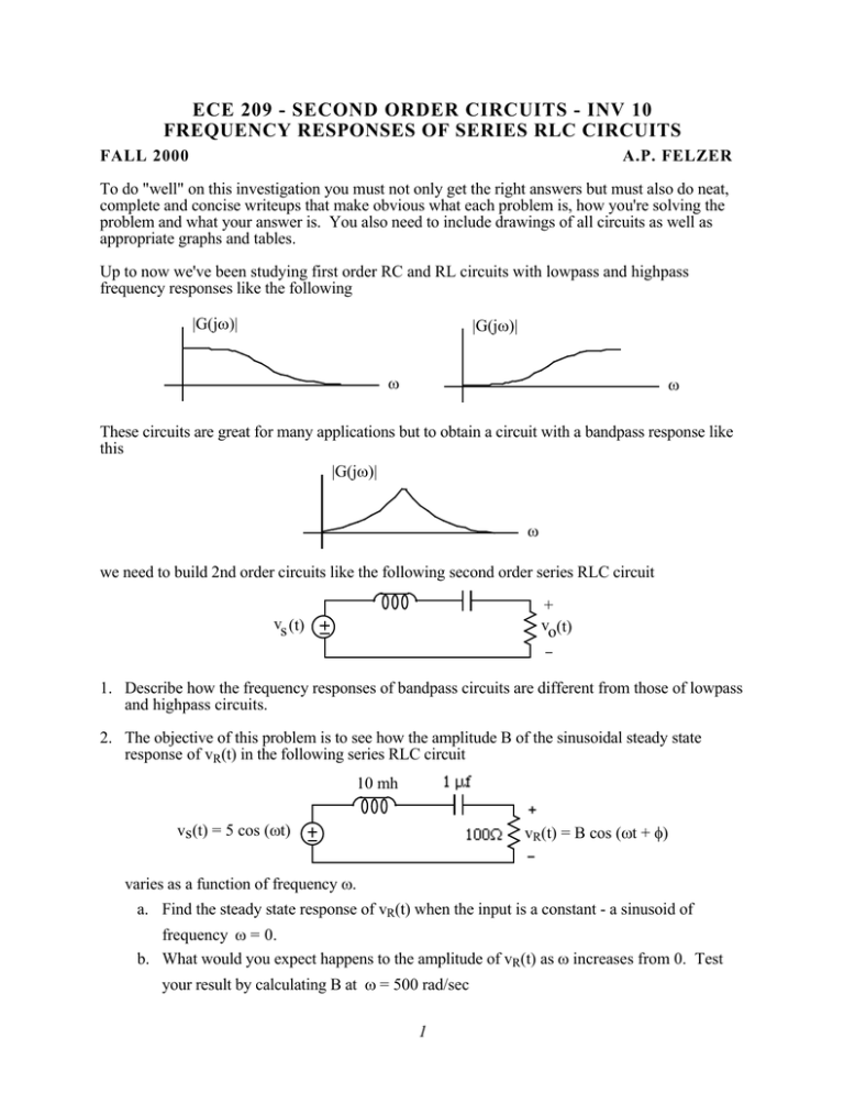
ECE 209 - SECOND ORDER CIRCUITS - INV 10 FREQUENCY RESPONSES OF SERIES RLC CIRCUITS FALL 2000 A.P. FELZER To do "well" on this investigation you must not only get the right answers but must also do neat, complete and concise writeups that make obvious what each problem is, how you're solving the problem and what your answer is. You also need to include drawings of all circuits as well as appropriate graphs and tables. Up to now we've been studying first order RC and RL circuits with lowpass and highpass frequency responses like the following |G(jω)| |G(jω)| ω ω These circuits are great for many applications but to obtain a circuit with a bandpass response like this |G(jω)| ω we need to build 2nd order circuits like the following second order series RLC circuit + vo(t) vs (t) 1. Describe how the frequency responses of bandpass circuits are different from those of lowpass and highpass circuits. 2. The objective of this problem is to see how the amplitude B of the sinusoidal steady state response of vR(t) in the following series RLC circuit 10 mh vR(t) = B cos (ωt + φ) vs(t) = 5 cos (ωt) varies as a function of frequency ω. a. Find the steady state response of vR(t) when the input is a constant - a sinusoid of frequency ω = 0. b. What would you expect happens to the amplitude of vR(t) as ω increases from 0. Test your result by calculating B at ω = 500 rad/sec 1 c. Find the steady state response of vR(t) when ω = ∞. d. Make use of your results in parts (a)-(c) to sketch |VR(jω)| as a function of frequency ω. Note that we refer to second order bandpass circuits like the one we've been analyzing in this problem as resonant circuits. 3. The objective of this problem is to calculate and sketch the transfer function 10 mh vR(t) = B cos (ωt + φ) vs(t) = A cos (ωt) of the bandpass circuit in Problem (2) as given by G( j ) = VR ( j ) Vs a. Find G(jω) = VR(jω)/Vs b. Use Mathcad to obtain a graph of |G(jω)| as a function of ω on a log scale c. Describe your graph in part (b) d. Reconcile any differences between your graphs in part (b) of this problem and part (d) in Problem (2) 4. Find the sinusoidal steady state response of a second order series RLC circuit with the following transfer function G( j ) = VR ( j ) 1000( j ) = 2 Vs (j ) + 1000( j ) + 10 6 to the input vs(t) = 5 cos (1000t) 5. The objective of this problem is to sketch graphs of what we would see on a scope as we increase the frequency in a series RLC resonant circuit like the one in Problems (2) and (3) with frequency responses as follows |G(jω)| = |VR(jω)/Vs| ω1 ω2 ω3 ω4 ω (log scale) a. Sketch vs(t) and the sinusoidal steady state response vR(t) at each of the frequencies ω = ω1 , ω2 , ω3 , ω4 . Put all sketches on separate graphs. b. Describe what's happening to the steady state response of vR(t) as ω increases from 0 6. The objective of this problem is to define what we mean by the resonance frequency ωp and what we mean by the 3dB bandwidth of a bandpass circuit. Given the following series RLC 2 circuit 0.01 µf 10 mh vs(t) 1K vR(t) with bandpass transfer function as follows G( j ) = VR ( j ) 105 (j ) = Vs (j ) 2 + 105 ( j ) + 1010 a. Use Mathcad to obtain a graph of |G(jω)| = |VR(jω)/Vs| versus ω on a log scale. b. Make use of your graph in part (a) to find the resonance frequency p - the frequency where the response is maximum. Note that a resonant circuit is said to be in resonance at the frequency ωp c. Make use of your graph in part (a) to find the lower and upper 3dB frequencies l3dB and of G(jω) d. Make use of your result in part (c) to find the 3dB Bandwidth as defined by 3dB BW = u 3dB − l 3dB u 3dB 7. The objective of this problem is to analyze a general 2nd order series RLC resonant circuit as given by L C vs(t) R vR(t) a. Verify that the voltage transfer function is G( j ) = VR ( j ) R R = = 1 1 Vs R+ j L + R + j L − j C C b. Use your result in part (a) to obtain a general expression for the resonant frequency ωp the frequency where |G(jω)| is maximum. Note that you don't have to take any derivates to find ωp. Since the numerator is constant, you only have to find where the denominator is minimum. c. Verify that your result in part (b) 1 p = LC gives the same value gives the same value for ωp as your graph in Problem (6) for the corresponding values of L and C. d. Verify that the impedance of a series LC circuit as follows 3 is equal to zero at resonance. Memorize this result. e. Given that the 3dB frequencies of a series RLC circuit are as follows 1 = − 2 R 1 R + + 2L 2L LC and 2 =+ 2 R 1 R + + 2L 2L LC find the 3dB Bandwidth = ω2 – ω1 . f. Verify that your result in part (e) gives the same value gives the same value for the 3dB Bandwidth as your graph in Problem (6) for the corresponding values of L and C. g. And finally - express the general equation in part (a) in standard form as follows K(j ) G( j ) = 2 ( j ) + a( j ) + b 8. The objective of this problem is to find the relation between vL(t) and vC(t) at resonance in series RLC circuits as follows vC(t) vL(t) i(t) vs(t) L C a. Find VL(jω) and VC(jω) in terms of I(jω) b. Make use of your result in part (a) to show that vL(t) and vC(t) are 180 degrees out of phase. c. Make use of your result in part (b) to sketch vL(t) and vC(t) on the same graph at a frequency ω < ωp d. Make use of your result in part (b) to sketch vL(t) and vC(t) on the same graph at a frequency ω = ωp e. Make use of your result in part (b) to sketch vL(t) and vC(t) on the same graph at a frequency ω > ωp f. Make use of your results in parts (c)-(e) to describe the relationship between vL(t) and vC(t) as ω increases from ω < ωp to ω > ωp 4
