A Novel DC-DC Boost Converter for Piezoelectric Actuators in
advertisement
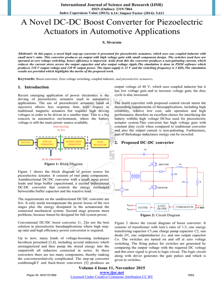
International Journal of Science and Research (IJSR) ISSN (Online): 2319-7064 Index Copernicus Value (2013): 6.14 | Impact Factor (2014): 5.611 A Novel DC-DC Boost Converter for Piezoelectric Actuators in Automotive Applications S. Sivaram Abstract: In this paper, a novel high step-up converter is presented for piezoelectric actuators, which uses one coupled inductor with small turn’s ratio. This converter produces an output with high voltage gain with small component design. The switches used here are operated at zero voltage switching, hence efficiency is improved. Aside from this the converter produces a non-pulsating current, which reduces the current stress across the output capacitor and also output voltage ripple.The simulation is done in PSIM software which produces 110 V output voltage and 120 W output power. The input supply is 12 V and the switching frequency is 5 KHz.The simulation results are provided which highlights the merits of the proposed work. Keywords: Boost converter, Zero voltage switching, coupled inductor, and piezoelectric actuators. 1. Introduction Recent emerging application of power electronics is the driving of piezoelectric actuators used in automotive applications. The use of piezoelectric actuators (used as injectors) allows less response time with respect to traditional magnetic actuators but requires high driving voltages in order to be driven in a smaller time. This is a big concern in automotive environment, where the battery voltage is still the main power source available. output voltage of 48 V, which uses coupled inductor but it has low voltage gain and to increase voltage gain, the duty cycle is also increased. The boost converter with proposed control circuit meets the demanding requirements of theseapplications, including high reliability, relative low cost, safe operation and high performance, therefore an excellent choice for interfacing the battery withthe high voltage DCbus used for piezoelectric actuator system.This converter has high voltage gain with constant duty cycle when compared to traditional converter and also the output current is non-pulsating. Furthermore, part of theleakage inductance energy can be recycled. 2. Proposed DC-DC converter Figure 1: Block Diagram Figure 1 shows the block diagram of power source for piezoelectric actuator. It consists of two main components. Aunidirectional DC/DC converter with a small input power loads and large buffer capacitorand, a second bidirectional DC/DC converter that controls the energy exchanged betweenthe buffer capacitor and the reactive load. The requirements on the unidirectional DC/DC converter are few. It only needs tocompensate the power losses of the two stages plus the energy dissipated in the actuatorand the connected mechanical system. Second stage presents more problems, because itmust be designed for full system power. Conventional DC/DC boost converter [1, 2]is not the best solution in piezoelectric basedapplications where high stepup ratio and high efficiency power conversion is required. Up to now, many kinds of voltage-boosting techniques havebeen presented [3,4], including several inductors which aremagnetized and then pump the stored energy into the outputwith all inductors connected in series. In these converters there are too many components, thereby making the convertersrelatively complicated. The step-up converter combiningKY and buck-boost converters [5] produces an Paper ID: NOV151569 Figure 2: Circuit Diagram Figure 2 shows the circuit diagram of boost converter. It consists of transformer with turn’s ratio of 1:3, one energy transferring capacitor C1,one charge pump capacitor C2, one diode D1, one outputinductor Lo, and one output capacitor Co. The switches are turned on and off at zero voltage switching. The firing pulses for switches are generated by comparing the output voltage with the required DC voltage and this error signal is given to logic circuit. The logic circuit along with driver generates the gate pulses and which is given to switches. Volume 4 Issue 11, November 2015 www.ijsr.net Licensed Under Creative Commons Attribution CC BY 1653 International Journal of Science and Research (IJSR) ISSN (Online): 2319-7064 Index Copernicus Value (2013): 6.14 | Impact Factor (2014): 5.611 The operating principles of the circuit can be explained in two modes. 2.1 Mode A Figure 3: Power flow in mode A Figure 3 shows the power flow diagram during mode A operation. In this mode gate pulse is given to switch 2, hence it will be turned on. The supply will appear across primary winding and hence a voltage is induced in the secondary which forward bias diode D1. The capacitor C2 starts charging and inductor Lo starts discharging. Figure 5 shows the waveform of gate pulse given to the switches, inductor voltage and inductor current during this mode of operation. The voltage across the inductor L0 is given as VLO = VC2 – VO (1) 2.2 Mode B Figure 5: Operating waveform 2.3 Design The value of the output inductor is calculated from the below equation and is given as Lo = 𝑉𝐿𝑜 ∆𝑡 ∆𝑖 𝐿𝑜 = (𝑉𝐶1 + 𝑉𝑖 +𝑉𝐶2 −𝑉𝑜 ) (1−𝐷)𝑇𝑆 ∆𝑖 𝐿𝑜 (3) The value of the energy transferring capacitor C1 is calculated from the below equation and is given as C1 = 𝑖 𝑐1 ∆𝑡 ∆𝑉𝑐1 = (𝐼𝑖 𝑟𝑎𝑡𝑒𝑑 −𝐼𝑜 𝑟𝑎𝑡𝑒𝑑 ) (1−𝐷)𝑇𝑆 ∆𝑉𝑐1 (4) 3. Simulation and Result Figure 4: Power flow in mode B Figure 4 shows the power flow diagram during mode B operation. In this mode gate pulse is given to switch 1, hence it will be turned on. The capacitor C1 imposes a negative voltage on primary winding and hence a voltage is induced in the secondary which reverse bias diode D1. The inductor Lo now starts charging.Figure 5 shows the waveform of gate pulse given to the switches, inductor voltage and inductor current during this mode of operation. The voltage across the inductor L0 is given as VLO = Vi + VC1 + VC2 – VO Paper ID: NOV151569 (2) Figure 6: PSIM simulation circuit Figure 6 shows the simulation circuit diagram of proposed circuit done in PSIM software. Volume 4 Issue 11, November 2015 www.ijsr.net Licensed Under Creative Commons Attribution CC BY 1654 International Journal of Science and Research (IJSR) ISSN (Online): 2319-7064 Index Copernicus Value (2013): 6.14 | Impact Factor (2014): 5.611 4. Conclusion Figure 7: Gate pulse waveform Figure 7 shows the gate pulse waveform generated for the switches. The switching frequency is 5 KHz and the duty cycle of operation is 0.5. A high voltage gain converter with high efficiency for piezoelectric actuators in automotive applications has been presented in this paper. Here the switches are turned on and off at zero voltage. Therefore switching losses are reduced and hence efficiency is improved when compared to traditional converters. The maximum voltage stress across the switch is small thereby reducing the size of the switches used. The duty ratio is maintained constant and is 0.5. Hence heat generated is reduced. The output voltage remains in constant voltage when there is a transient in load. References Figure 8: Output voltage and current waveform Figure 8 shows the output voltage and current waveform of the converter. It produces an output voltage of 110 V and current of 1.1 A. The load current is not pulsating. [1] Abrahan I. Pressman, Switching Power Supply Design, 2nd ed., New York:McGraw-Hill, 1998. [2] R. W. Erickson and D. Maksimovic, Fundamentals of Power Electronics, 2nd ed., Norwell: KLuwer Academic Publishers, 2001. [3] B. R. Lin, F. Y. Hsieh and J. J. Chen, “Analysis and implementation of a bidirectional converter with high converter ratio,” IEEE ICIT’08, pp.1-6, 2008. [4] F. L. Luo, “Analysis of super-lift luo-converters with capacitor voltage drop,” IEEE ICIEA’ 08, pp. 417-422, 2008. [5] K. I. Hwu, K. W. Huang and W. C. Tu, “Step-up convertercombining KY and buck-boostconverters,” IET ElectronicsLetters, vol. 47, no. 12, pp. 722-724, 2011. Figure 9: Gate pulse and Switch voltage Figure 9 shows the gate pulse and switch voltage waveform of the switch 1. The switches are turned on and off at zero voltage, therefore the switching losses are reduced and thereby increasing the efficiency. The maximum voltage stress across the switch is only 12 V. hence the cost and size is also reduced. Figure 10:Transient load current waveform Figure10 shows the load current waveform during transient operation. It is clear that the output voltage of the converter is stable when the load current changes from 1.1 A to 1.8 A and vice versa. Paper ID: NOV151569 Volume 4 Issue 11, November 2015 www.ijsr.net Licensed Under Creative Commons Attribution CC BY 1655

