A 6kV/5kA Reverse Conducting GCT
advertisement

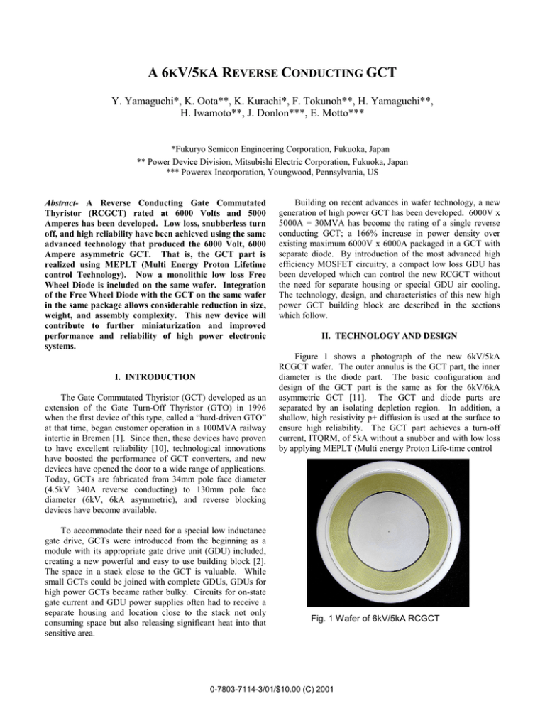
A 6KV/5KA REVERSE CONDUCTING GCT Y. Yamaguchi*, K. Oota**, K. Kurachi*, F. Tokunoh**, H. Yamaguchi**, H. Iwamoto**, J. Donlon***, E. Motto*** *Fukuryo Semicon Engineering Corporation, Fukuoka, Japan ** Power Device Division, Mitsubishi Electric Corporation, Fukuoka, Japan *** Powerex Incorporation, Youngwood, Pennsylvania, US Abstract- A Reverse Conducting Gate Commutated Thyristor (RCGCT) rated at 6000 Volts and 5000 Amperes has been developed. Low loss, snubberless turn off, and high reliability have been achieved using the same advanced technology that produced the 6000 Volt, 6000 Ampere asymmetric GCT. That is, the GCT part is realized using MEPLT (Multi Energy Proton Lifetime control Technology). Now a monolithic low loss Free Wheel Diode is included on the same wafer. Integration of the Free Wheel Diode with the GCT on the same wafer in the same package allows considerable reduction in size, weight, and assembly complexity. This new device will contribute to further miniaturization and improved performance and reliability of high power electronic systems. I. INTRODUCTION The Gate Commutated Thyristor (GCT) developed as an extension of the Gate Turn-Off Thyristor (GTO) in 1996 when the first device of this type, called a “hard-driven GTO” at that time, began customer operation in a 100MVA railway intertie in Bremen [1]. Since then, these devices have proven to have excellent reliability [10], technological innovations have boosted the performance of GCT converters, and new devices have opened the door to a wide range of applications. Today, GCTs are fabricated from 34mm pole face diameter (4.5kV 340A reverse conducting) to 130mm pole face diameter (6kV, 6kA asymmetric), and reverse blocking devices have become available. To accommodate their need for a special low inductance gate drive, GCTs were introduced from the beginning as a module with its appropriate gate drive unit (GDU) included, creating a new powerful and easy to use building block [2]. The space in a stack close to the GCT is valuable. While small GCTs could be joined with complete GDUs, GDUs for high power GCTs became rather bulky. Circuits for on-state gate current and GDU power supplies often had to receive a separate housing and location close to the stack not only consuming space but also releasing significant heat into that sensitive area. Building on recent advances in wafer technology, a new generation of high power GCT has been developed. 6000V x 5000A = 30MVA has become the rating of a single reverse conducting GCT; a 166% increase in power density over existing maximum 6000V x 6000A packaged in a GCT with separate diode. By introduction of the most advanced high efficiency MOSFET circuitry, a compact low loss GDU has been developed which can control the new RCGCT without the need for separate housing or special GDU air cooling. The technology, design, and characteristics of this new high power GCT building block are described in the sections which follow. II. TECHNOLOGY AND DESIGN Figure 1 shows a photograph of the new 6kV/5kA RCGCT wafer. The outer annulus is the GCT part, the inner diameter is the diode part. The basic configuration and design of the GCT part is the same as for the 6kV/6kA asymmetric GCT [11]. The GCT and diode parts are separated by an isolating depletion region. In addition, a shallow, high resistivity p+ diffusion is used at the surface to ensure high reliability. The GCT part achieves a turn-off current, ITQRM, of 5kA without a snubber and with low loss by applying MEPLT (Multi energy Proton Life-time control Fig. 1 Wafer of 6kV/5kA RCGCT 0-7803-7114-3/01/$10.00 (C) 2001 Technology). The diode part achieved a reduction in loss of approximately 70% by applying a p+ structure on the n+ side of a conventional PIN structure. Details of the this diode design can be found in the ISPSD2000 paper by our coworkers [13]. Figure 2 shows the cross-section of the GCT unit cell, diode, and separation region. Figure 3 shows the effect of the MEPLT process on the different structure levels of the GCT. Gate Al Cathode Al Cathode Al NE PB P III. CHARACTERISTICS Figure 4 shows the snubberless turn-off waveforms of the new RCGCT at anode current IT = 5kA, bus voltage VD = 3.0kV, and junction temperature TJ = 25°C. Figure 5 shows a typical snubberless turn-off of the integrated diode at load current IT = 2800A, dIT/dt = 500 A/µs, bus voltage VD = 3000V, and TJ = 125°C. Figures 6 and 7 show typical Eoff and Erec losses as a function of anode current IT and bus voltage VD. Table 1 summarizes the main characteristics of the new RCGCT: Small GCT loss in on-state and switching, small diode loss especially at reverse recovery, and low thermal resistance. Additionally, the peak off-state current is reduced considerably in comparison to a GCT diode combination, making the new device a good choice for series connection. N- PE P N+ Anode Al N+ + Diode Part (Inner Side) Separation Part GCT Part (Outer Side) Fig. 2 Cross-section of GCT unit cell, diode, and separation region NE PB PB Proton Energy Small 1 2 Proton Energy large N- PE 3 N+ Proton Energy Small Relative Comparison of Proton Dose Section Note: Recovery characteristic Loss Snap 1 + + 2 + 3 / ‘ + ’ has a beneficial good effect ‘ - ‘ has a detrimental effect ‘ / ’ has no effect Turn-off characteristic Loss / + + The p+ structure improves these. Fig. 3 MEPLT Process effects 0-7803-7114-3/01/$10.00 (C) 2001 ts=2µs IT=5000A VD=3000V Fig. 4 Snubberless Turn-off Waveform Fig. 5 Snubberless Diode Turn-off Waveform Eof f vs IT, VD Ere c vs IF,VR Typical Typic a l 25 5 Condition: Condit ion: Tj =125deg 20 Cc =6uF VD3000V Tj =125de g 4 Lc =0. 4uH Cc =6uF Lc =0.4uH 3 VD 2000V Erec [J] Eoff [J] 15 VD 1000V 10 VR 3000V AL =5.7uH VR 2000V 2 1 5 VR 1000V 0 0 0 0 1000 2000 3000 4000 1000 2000 Fig. 8 New GDU with GC GCT 4000 IF [ A] IT [A] Fig. 6 Eoff vs. IT, VD 3000 5000 Fig. 7 Erec vs. IT, VD Fig. 9: Total power consumption (dashed lines) and power loss (solid lines) of the new GDU in 2-level operation. Curves are shown for switching frequency fs =100Hz, 200Hz and 500Hz at duty = 50%. 0-7803-7114-3/01/$10.00 (C) 2001 Table 1 Main Characteristics Item Characteristics Condition Controllable VD=3000V 5000A turn-off current diGQ/dt=10000A/µs Peak off-state >6000V VGR=-2V voltage Peak off-state 100mA VDM=6000V, Tj=125°C current Peak reverse 10mA VRG=21V, Tj=125°C current Eon 0.4J/P IT=2800A, VD=3000V Eoff 12J/P IT=2800A, VD=3000V Erec 2.5J/P IT=2800A, VD=3000V On-state voltage 3.0V IT=2800A,Tj=125°C Forward voltage 4.5V IF=2800A,Tj=125°C Rth GCT part 0.0075°C/W ― Diode part 0.0082°C/W Table 2 Features of Selected High Power Devices Peak off-state voltage Controllable turn-off current DC voltage for 100 FIT Peak off-state current GCT on-state voltage @ IT Diode forward voltage @ IT Eon @ IT, VD Eoff @ IT Erec @ IF Rthj-c GCT/IGBT part Rthj-c Diode part Rthc-heatsink GCT/IGBT part Rthc-heatsink Diode Rth heatsink GCT/IGBT Rth heatsink Diode 6” RCGCT 6000V 5000A 3600V 100mA 3.0 V @ 2800A 4.5 V @ 2800A 0.4 J/P @ 2800A, 3kV 12 J/P @ 2800A, 3kV 2.5 J/P @ 2800A, 3kV 7.5 K/kW 8.2 K/kW 2 K/kW 2 K/kW 7 K/kW 6.5 K/kW 4” GCT 6000V 4000A 3600V 3.8V @ 4000A 15 J/P @ 4000A, 3kV 10 K/kW 3 K/kW 8 K/kW IGBT module 4500V 1800A (2*900A) 2800V 90mA 4.2V @ 1500A 4.8V @ 1500A 2.2 J/P @ 500A, 2250V 1.8 J/P @ 500A, 2250V 0.66 J/P @ 500A, 2250V 10 K/kW 20 K/kW 10.5 K/kW 21 K/kW 8 K/kW 16 K/kW 3-phase 2-level Inverter Operation VDC-link, 500Hz Irms, cos Φ = 1 Pout, cos Φ = 1 Irms, cos Φ = -1 Pout, cos Φ = -1 3600V 1900A 9.2MW 1740A 8.25MW * Pole piece diameter of 6” RCGCT is 130mm 3600V 1760A 8.46MW 2250V 860A 2.58MW 810A 2.43MW ** Mitsubishi IGBT module CM900HB-90H footprint is 190mm x 140mm. A new low loss Gate Drive Unit was developed for the RCGCT [14]. Figure 8 shows the Turn-on/Turn-off part of the new GDU with the RCGCT. The IGon, low pulse, control, and power supply section is mounted on top of the Turn-on/Turn-off circuit creating a very compact GDU. 0-7803-7114-3/01/$10.00 (C) 2001 The new GDU achieves low power consumption as shown in Figure 9. A large fraction of this power is transferred to the GCT and a total loss of less than 12W is expected. Table 2 presents a comparative overview of the main features various actual high power devices. The output capability of a 3-phase 2-level inverter using each of these devices is shown in the lower part of the table. The inverter operation is based on assumptions of inlet water temperature TW = 40°C, operating junction temperature of TJ=125°C, and all devices cooled using a very efficient all copper heat sink. It is seen that the new 6 inch RCGCT provides a well balanced set of characteristics for the highest output capability. The Integration of the Free Wheel Diode with the GCT on the same wafer in the same package allows considerable reduction in size, weight, and assembly complexity. This can be envisioned by examining the three schematic implementations of one phase of a voltage source inverter using a reverse blocking GTO, a reverse blocking GCT, and the new reverse conducting GCT as shown in Figure 10. The significant reduction in component count is apparent. Figures 11 and 12 then show the actual size and weight reduction achievable with the new Reverse Conducting GCT. IV. CONCLUSION A new power electronic building block – RCGCT and GDU – has been developed. It combines high turn-off capability and low loss and is specially dedicated to high power applications like steel rolling mill drives, SVC, UPFC, and interties. This new building block will further enhance compactness, reliability, and modularity of high power electronic systems. [5] Data Sheet of Gate Driver GU-C40, Mitsubishi Electric Corporation, Aug. 1998. [6] K. Satoh, et al., “6kV/4kA Gate Commutated Turn-Off Thyristor with Operation DC Voltage at 3.6kV”, ISPSD 1998. [7] K. Kurachi, et al., “GCT Thyristor – A Novel Approach to High Power Conversion”, PCIM Inter 1998. [8] M. Yamamoto, et. al., “GCT Thyristor and Gate Drive Circuit”, PESC 1998. [9] J.F. Donlon, E.R. Motto, M. Yamamoto, T. Iida, “A New Gate Commutated Turn-Off Thyristor and Companion Diode for High Power Applications”, IEEE IAS Conference 1998, pp. 873-880. [10] H. Gruening, D. Leonard, “Leistungshalbleiter und Schaltungstechnik fuer Bahnstromanwendungen der Zukunft”, Elektrische Bahnen 97, R. Oldenburg Verlag 1999, Vol. 1-2, pp. 42-48. [11] K. Satoh, K. Morishita, Y. Yamaguchi, H. Hirano, H. Iwamoto, A. Kawakami, “New Design Approach For Ultra High Power GCT Thyristor“, Proceedings of IEEE ISPSD 1999, pp. 351-354. [12] M. Mukunoki, K. Takao, H. Yamaguchi, Y. Shimomura, F. Mizohata, S. Mizoguchi, M. Koyama, “Highefficiency large-capacity three-level GCT Inverter”, IEEJ Conference Proceedings SPC-00-43, 2000, pp. 35-40. [13] K. Satoh, K. Morishita, Y. Yamaguchi, N. Hirano, H. Iwamoto, A. Kawakami, “A Newly Structured High Voltage Diode Highlighting Oscillation Free Function In Recovery Process”, Proceedings of the ISPSD 2000, pp. 249-252 [14] H. Gruening, T. Tsuchiya, K. Satoh, Y. Yamaguchi, F. Mizohata, K. Takao, “6kV 5kA RCGCT with Advanced Gate Drive Unit”, Proceedings of the ISPSD 2001, pp. 133-136. REFERENCES [1] P.K.Steimer, H. Gruening, J. Werninger, D. Schroeder, “State-of-the-Art Verification of the Hard Driven GTO Inverter Development for a 100 MVA Intertie”, Proceedings of IEEE PESC, Baveno, 1996, pp. 14011407 [2] H. Gruening, B. Oedegard, A. Weber, E. Carroll, S. Eicher, “High Power Hard-Driven GTO Module for 4.5 kV/3kA Snubberless Operation,” in Conf. Rec, PCIM’96, 1996, pp. 169-183 [3] K. Satoh, et al. , “A New High Power Device GCT (Gate Commutated Turn-off) Thyristor”, EPE 1997 [4] M. Matsushita, T. Ogura, I. Omura, N. Ninomiya, H. Ohashi, Realizing High Frequency Operation”, ISPSD 1997, pp. 247-250. 0-7803-7114-3/01/$10.00 (C) 2001 Snubber circuit C lamp circuit R DGTO RDGC T FR D RD GTO RCGCT RCGCT Type ( RD GC T Type FG6000AU -120DA FGC 6000AX -120DS FGC R5000AX -120DS Fig. 10 Implementations of a Voltage Source Inverter Phase Device Volum e 1400 1200 Diode + RDGCT type Volume [cm3] 1000 800 600 400 RCGCT type 200 0 0 5 10 15 Fig. 11 20 M VA 25 Device Volume vs. Power Output 0-7803-7114-3/01/$10.00 (C) 2001 30 35 40 Device W eight 7 6 Weight [Kg] 5 Diode + RDGCT type 4 3 RCG CT type 2 1 0 0 5 10 15 Fig. 12 20 M VA 25 Device Weight vs. Power Output 0-7803-7114-3/01/$10.00 (C) 2001 30 35 40


