Circuit Note
CN-0277
Devices Connected/Referenced
Circuits from the Lab™ reference circuits are engineered and
tested for quick and easy system integration to help solve today’s
analog, mixed-signal, and RF design challenges. For more
information and/or support, visit www.analog.com/CN0277.
AD7960
18-Bit, 5 MSPS PulSAR® Differential ADC
ADA4897-1/
ADA4897-2
1 nV/√Hz, Low Power, Rail-to-Rail
Output Single/Dual Amplifiers
AD8031/
AD8032
2.7 V, 800 μA, 80 MHz Rail-to-Rail I/O
Single/Dual Amplifiers
ADR4550
Ultralow Noise, High Accuracy Voltage
References
High-Precision, 18-Bit, 5 MSPS, Low Power Data Acquisition Signal-Chain
EVALUATION AND DESIGN SUPPORT
CIRCUIT FUNCTION AND BENEFITS
Circuit Evaluation Boards
AD7960 Circuit Evaluation Board (EVAL-AD7960FMCZ)
System Demonstration Platform (EVAL-SDP-CH1Z)
Design and Integration Files
Schematics, Layout Files, Bill of Materials
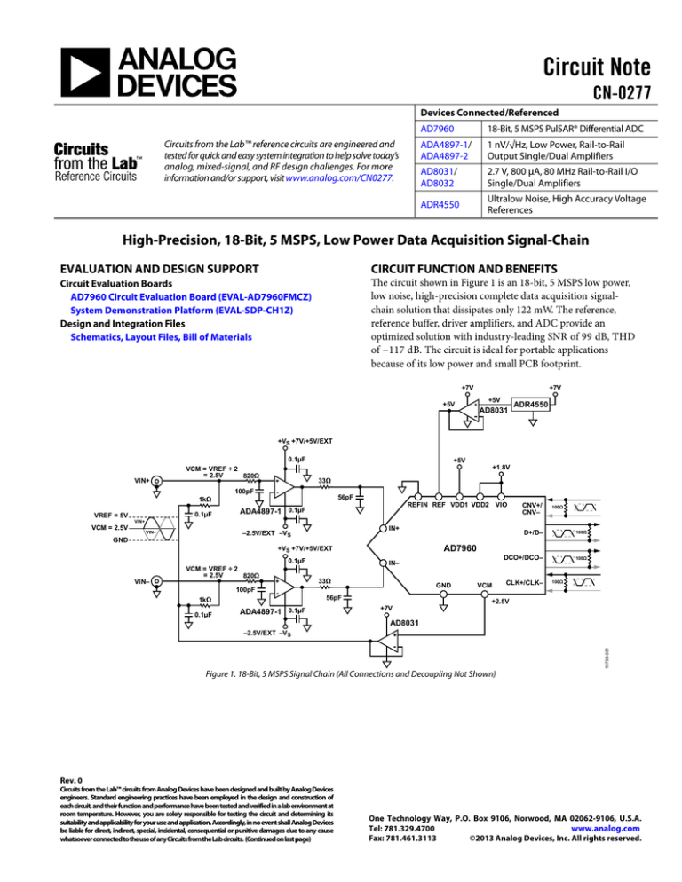
The circuit shown in Figure 1 is an 18-bit, 5 MSPS low power,
low noise, high-precision complete data acquisition signalchain solution that dissipates only 122 mW. The reference,
reference buffer, driver amplifiers, and ADC provide an
optimized solution with industry-leading SNR of 99 dB, THD
of −117 dB. The circuit is ideal for portable applications
because of its low power and small PCB footprint.
+7V
+5V
+7V
+5V
AD8031
ADR4550
+VS +7V/+5V/EXT
0.1µF
VIN+
VCM = VREF ÷ 2
= 2.5V
820Ω
+5V
100pF
56pF
1kΩ
VREF = 5V
VCM = 2.5V
0.1µF
+1.8V
33Ω
REFIN REF VDD1 VDD2 VIO
ADA4897-1 0.1µF
CNV+/
CNV–
100Ω
VIN+
IN+
–2.5V/EXT –VS
VIN–
GND
VIN–
VCM = VREF ÷ 2
= 2.5V
820Ω
IN–
33Ω
GND
100pF
56pF
1kΩ
0.1µF
ADA4897-1 0.1µF
100Ω
DCO+/DCO–
100Ω
AD7960
+VS +7V/+5V/EXT
0.1µF
D+/D–
+7V
VCM
CLK+/CLK–
100Ω
+2.5V
AD8031
10798-001
–2.5V/EXT –VS
Figure 1. 18-Bit, 5 MSPS Signal Chain (All Connections and Decoupling Not Shown)
Rev. 0
Circuits from the Lab™ circuits from Analog Devices have been designed and built by Analog Devices
engineers. Standard engineering practices have been employed in the design and construction of
each circuit, and their function and performance have been tested and verified in a lab environment at
room temperature. However, you are solely responsible for testing the circuit and determining its
suitability and applicability for your use and application. Accordingly, in no event shall Analog Devices
be liable for direct, indirect, special, incidental, consequential or punitive damages due to any cause
whatsoever connected to the use of any Circuits from the Lab circuits. (Continued on last page)
One Technology Way, P.O. Box 9106, Norwood, MA 02062-9106, U.S.A.
Tel: 781.329.4700
www.analog.com
Fax: 781.461.3113
©2013 Analog Devices, Inc. All rights reserved.
CN-0277
Circuit Note
The input signals to the ADA4897-1 op amps are filtered by the
820 Ω/ 100 pF network that has a bandwidth of 2 MHz. Additional
filtering at the input of the AD7960 ADC is provided by the 33 Ω/
56 pF network that has a bandwidth of 86 MHz. The latter filter
helps to reduce the kick back coming from the cap DAC input of
the AD7960 and limits the noise coming to the AD7960 inputs.
1.00
The circuit uses supplies of +7 V and −2.5 V for the input
ADA4897-1 drivers to minimize power dissipation and to achieve
the optimum system distortion performance. The ADA4897-1
output stage is rail-to-rail and swings to within 150 mV of each
supply rail. The additional headroom afforded by the +7 V and
−2.5 V supplies provides excellent distortion performance.
The AD7960 digital interface uses low voltage differential
signaling (LVDS) to enable high data transfer rates. An LVDS
CLK+/CLK− signal must be applied to the AD7960 to transfer
data to the digital host.
0.50
0.25
INL (LSB)
The AD7960 differential input range is set by a 5 V or 4.096 V
external reference voltage. In Figure 1, the 5 V reference is supplied
by the ADR4550 is a high precision, low power (max 950 µA
operating current), low noise voltage reference featuring ±0.02%
maximum initial error, excellent temperature stability, and low
output noise. The AD8031 is used to buffer the external reference
and the common-mode output voltage of the AD7960, and is
an ideal for a wide range of applications, from battery-operated
systems with large bandwidth to high-speed systems where
component density requires lower power dissipation. The AD8031
is also stable for large capacitive loads, and can drive the
decoupling capacitors that are required to minimize voltage
spikes caused by transient currents.
0.75
0
–0.25
–0.50
–0.75
–1.00
0
50000
100000
150000
200000
250000
CODE
10798-002
The ADA4897-1 is an ideal candidate for driving the AD7960
high precision 18-bit, 5 MSPS SAR ADC. The ADA4897-1 is a
low noise (1 nV/√Hz typical) and low power (3 mA) rail-to-rail
output amplifier that has 230 MHz bandwidth, 120 V/μs slew
rate, and settles to 0.1% in 45 ns.
The AD7960 converts the differential voltage of the antiphase
analog inputs (IN+ and IN−) into a digital output. The analog
inputs, IN+ and IN−, require a common-mode voltage equal to
one-half the reference voltage. The low noise and low power
AD8031 amplifier buffers the +5V reference voltage from the
low noise and low drift ADR4550 and it also buffers the commonmode output voltage (VCM) of the AD7960. The ADA4897-1 is
configured as a unity gain buffer and drives the inputs of the
AD7960 with a 0 V to 5 V differential anti-phase (180°out of
phase with each other). Figure 2 shows the typical integral
nonlinearity as a function of the AD7960 output code is within
the specifications of ±0.8 LSB using a 5 V external reference.
Figure 2. AD7960 Typical Integral Nonlinearity vs. Output Code, REF = 5 V
Histogram and FFT Performance
The precision performance of the circuit shown in the histogram
plot in Figure 3 and the FFT plot in Figure 4 using a 5 V external
reference . The data was taken using the EVAL-AD7960FMCZ
evaluation board and the Audio Precision SYS-2702 as a signal
source.
The AD7960, 5MSPS, 18-bit converter has ±0.8 LSB INL, ±0.5 LSB
DNL, 100 dB DR, and dissipates only 46.5 mW. As shown in
Figure 1, the AD7960 is powered from +5 V (VDD1) and +1.8 V
(VDD2 and VIO) supplies. The required 5 V and 1.8 V supplies
can be generated using LDOs such as ADP7104 and ADP124.
14000
13000
12000
11000
OCCURRENCES
CIRCUIT DESCRIPTION
10000
9000
8000
7000
6000
6000
Figure 3. Typical Histogram, REF = 5 V
Rev. 0 | Page 2 of 5
65000
60000
10798-003
BINS
55000
50000
45000
40000
35000
30000
25000
20000
15000
10000
0
5000
4000
Circuit Note
CN-0277
0
–20
–40
AMPLITUDE (dB)
voltage noise, high speed op amp can be used instead of the
ADA4897-1 in the circuit if desired.
REFERENCE = 5V
INPUT FREQENCY = 1kHz
SNR = 96.5dB
SINAD = 96dB
THD = –111.5dB
SFDR = 113.1dB
–60
CIRCUIT EVALUATION AND TEST
The EVAL-AD7960FMCZ evaluation board was developed to
evaluate and test the AD7960 ADC. To test the circuit shown in
Figure 1, two ADA4897-1 op amps were used to drive the AD7960.
–80
–100
A detailed schematic and user instructions are available in the
EVAL-AD7960FMCZ user guide UG-490. This documentation
describes how to run the ac/dc tests described in this circuit note.
–120
–140
Note that the user has the option to provide +7 V and −2.5 V
supplies for the input amplifiers on the EVAL-AD7960FMCZ
board from the external dual power supply.
–180
0
0.5
1.0
1.5
2.0
FREQUENCY (MHz)
2.5
10798-004
–160
Figure 4. 1 kHz, −0.5 dBFS Input Tone FFT, REF = 5 V
Complete schematics and layout of the printed circuit board can
be found in the CN-0277 Design Support Package:
www.analog.com/CN0277-DesignSupport .
A functional block diagram of the test setup is shown in Figure 5,
and a photograph of the evaluation board is shown in Figure 6
Equipment Required
The following equipment is required to test the circuit:
COMMON VARIATIONS
The AD7961 is a 16-bit, 5 MSPS PulSAR® differential ADC and
is pin compatible with the AD7960 PulSAR® family, so it can be
used instead of the AD7960 in the circuit of Figure 1 when only
16-bit performance is required. The AD7960 series supports either
4.096 V or 5 V external references. The EVAL-AD7960FMCZ
board allows either the ADR4540 (4.096 V) or the ADR4550
(5 V) to be selected with a jumper.
The various options for connecting the reference voltage are
controlled by the enable EN[0:3] pins of the AD7960 as described
in the AD7960 datasheet. If a 0 V to 5 V input range is required,
the ADR4550 reference can be used with the AD8031 reference
buffer. This is done by setting the enable pins of the AD7960 as
EN[0:3] = ‘X001’ or ‘X101’.
The ADA4897-1 and AD8031 single op amps can be replaced
with their dual versions (ADA4897-2 and AD8032, respectively) if
desired.
For optimized noise and distortion performance, the ADA4899-1
(15 mA), unity-gain stable, ultralow distortion, 1 nV/√Hz
Rev. 0 | Page 3 of 5
The EVAL-AD7960FMCZ Evaluation Board and
Software
The System Demonstration Platform (EVAL-SDPCH1Z) board
A low distortion signal generator, such as the Agilent
81150A or Audio Precision SYS2702
A PC with a USB 2.0 port running Windows® XP,
Windows Vista, or Windows 7 (32-bit or 64-bit)
A 12 V dc wall wart (included with EVAL-SDP-CH1Z
board)
USB interface Cable (1) and SMA cable (1)
CN-0277
Circuit Note
+12V
WALL WART
ADP7102
+5V
ADP7104
+12V
ADP2300
+12V
+7V
PC
(USB)
USB PORT
–VS = –2.5V
ADR4550
+7V
+5V
POWER
SUPPLY
CIRCUITRY
ADP124
+5V
AD8031
+1.8V
+VS
REFIN
AIN+
REF
VDD1
VDD2
VIO
CNV± 100Ω
AD4897-1
ADSP-BF522
–VS
IN+
D±
100Ω
AD7960
SIGNAL
GENERATOR
+7V
AUDIO
PRECISION
SYS-2702
AD4897-1
AIN–
–VS
VCM
LVDS
INTERFACE
DCO±
IN–
GND
VCM
SPARTAN-6
FPGA
XC6SLX25
100Ω
CLK± 100Ω
2.5V
+7V
AD8031
EVAL-AD7960FMCZ
EVAL-SDP-CH1Z
10798-005
160-PIN
10mm
VITA 57 CONNECTOR
Figure 5. Functional Diagram of Test Setup
TO +12V WALL WART
SMA
CONNECTOR
USB
PC
10798-006
SIGNAL SOURCE
Figure 6. EVAL-AD7960FMCZ Board Connected to EVAL-SDP-CH1Z Board
Rev. 0 | Page 4 of 5
Circuit Note
CN-0277
REVISION HISTORY
LEARN MORE
8/13—Revision 0: Initial Version
CN-0277 Design Support Package:
www.analog.com/CN0277-DesignSupport
CN-0307 Circuit Note, A 16-Bit, 6 MSPS SAR ADC System with
Low Power Input Drivers and Reference Optimized for
Multiplexed Applications
CN-0237 Circuit Note, Ultralow Power, 18-Bit, Differential
PulSAR® ADC Driver.
MT-031 Tutorial, Grounding Data Converters and Solving the
Mystery of AGND and DGND. Analog Devices.
MT-035 Tutorial, Op Amp Inputs, Outputs, Single-Supply, and
Rail-to-Rail Issues. Analog Devices.
MT-101 Tutorial, Decoupling Techniques. Analog Devices.
Voltage Reference Wizard Design Tool.
User Guide UG-490 for EVAL-AD7960FMCZ
User Guide for EVAL-SDP-CH1Z
Data Sheets and Evaluation Boards
AD7960 Data Sheet and Evaluation Board
ADA4897-1 Data Sheet
ADA4897-2 Data Sheet
ADR4550 Data Sheet
AD8031 Data Sheet
AD8032 Data Sheet
(Continued from first page) Circuits from the Lab circuits are intended only for use with Analog Devices products and are the intellectual property of Analog Devices or its licensors. While you
may use the Circuits from the Lab circuits in the design of your product, no other license is granted by implication or otherwise under any patents or other intellectual property by
application or use of the Circuits from the Lab circuits. Information furnished by Analog Devices is believed to be accurate and reliable. However, Circuits from the Lab circuits are supplied
"as is" and without warranties of any kind, express, implied, or statutory including, but not limited to, any implied warranty of merchantability, noninfringement or fitness for a particular
purpose and no responsibility is assumed by Analog Devices for their use, nor for any infringements of patents or other rights of third parties that may result from their use. Analog Devices
reserves the right to change any Circuits from the Lab circuits at any time without notice but is under no obligation to do so.
©2013 Analog Devices, Inc. All rights reserved. Trademarks and
registered trademarks are the property of their respective owners.
CN10798-0-8/13(0)
Rev. 0 | Page 5 of 5

