Evaluation Board for ADG824, 0.5 Ω CMOS,
1.65 V to 3.6 V, Dual SPDT/2:1 Mux in Mini LFCSP
EVAL-ADG824
The evaluation kit contains a fully fitted PCB and a CD that
contains the ADG824 data sheet and the EVAL-ADG824 data
sheet. Refer to the ADG824 data sheet for full data on the part.
Consult the ADG824 data sheet in conjunction with this data
sheet when using the evaluation board.
FEATURES
Full featured evaluation board for the ADG824
On-board audio connectors
GENERAL DESCRIPTION
CONNECTING SIGNALS TO THE BOARD
This data sheet describes the evaluation board for the ADG824,
which is a low voltage CMOS device that contains two
independently selectable, single-pole, double-throw (SPDT)
switches. The ADG824 offers ultralow on resistance of less than
0.7 Ω over the full temperature range.
The board is fitted with three audio connectors that allow
switching between audio devices. All signals applied to the switch
can be monitored using the test points provided on the board.
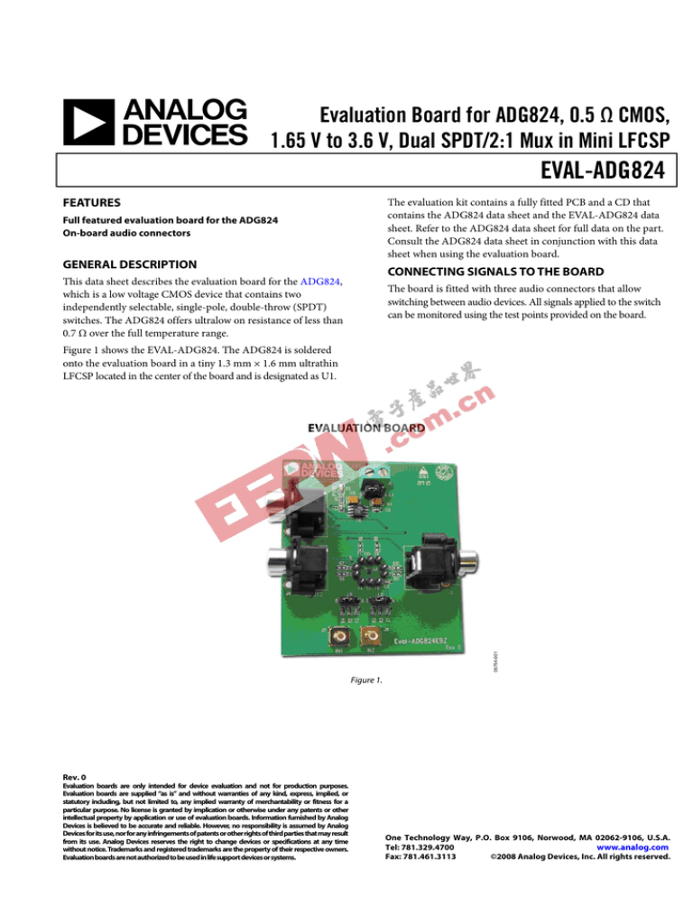
Figure 1 shows the EVAL-ADG824. The ADG824 is soldered
onto the evaluation board in a tiny 1.3 mm × 1.6 mm ultrathin
LFCSP located in the center of the board and is designated as U1.
06754-001
EVALUATION BOARD
Figure 1.
Rev. 0
Evaluation boards are only intended for device evaluation and not for production purposes.
Evaluation boards are supplied “as is” and without warranties of any kind, express, implied, or
statutory including, but not limited to, any implied warranty of merchantability or fitness for a
particular purpose. No license is granted by implication or otherwise under any patents or other
intellectual property by application or use of evaluation boards. Information furnished by Analog
Devices is believed to be accurate and reliable. However, no responsibility is assumed by Analog
Devices for its use, nor for any infringements of patents or other rights of third parties that may result
from its use. Analog Devices reserves the right to change devices or specifications at any time
without notice. Trademarks and registered trademarks are the property of their respective owners.
Evaluation boards are not authorized to be used in life support devices or systems.
One Technology Way, P.O. Box 9106, Norwood, MA 02062-9106, U.S.A.
www.analog.com
Tel: 781.329.4700
Fax: 781.461.3113
©2008 Analog Devices, Inc. All rights reserved.
EVAL-ADG824
TABLE OF CONTENTS
Features .............................................................................................. 1 Evaluation Board Schematics...........................................................4 General Description ......................................................................... 1 ADG824 Switch Pins, Test Points, and Connections ...............5 Connecting Signals to the Board .................................................... 1 PCB Drawings ....................................................................................6 Evaluation Board .............................................................................. 1 Ordering Information .......................................................................8 Revision History ............................................................................... 2 Component’s List ...........................................................................8 Hardware Description ...................................................................... 3 Ordering Guide .............................................................................8 Power Supply ................................................................................. 3 ESD Caution...................................................................................8 Switch Control Connectors ......................................................... 3 REVISION HISTORY
6/08—Revision 0: Initial Version
Rev. 0 | Page 2 of 8
EVAL-ADG824
HARDWARE DESCRIPTION
ADG824 EVALUATION BOARD
AUDIO
DEVICE 1
TO AUDIO
DEVICE 1
TO AUDIO
DEVICE 3
ADG824
AUDIO
DEVICE 2
TO AUDIO
DEVICE 2
AUDIO
DEVICE 3
CONTROL SECTION:
SWITCHES CAN BE CONTROLLED
MANUALLY BY CHANGING JUMPER
POSITIONS OR FROM AN EXTERNAL
SIGNAL SOURCE TO THE
SMB CONNECTORS.
L2
06754-002
L3
SMB CONNECTORS
Figure 2. Evaluation Board Block Diagram
The ADG824 evaluation kit contains a fully fitted PCB and a
CD that contains the ADG824 data sheet and the EVAL-ADG824
data sheet.
The evaluation board allows the user to switch between two
audio sources or to switch an audio source between two
speakers by using the on-board jumpers or by applying the
correct control signals to the appropriate connectors. The
following sections describe in detail the function of the
connectors and links.
POWER SUPPLY
For convenience, a regulator supplies the ADG824 with a 3.3 V
supply. A supply range of 3.3 V to 12 V can be connected to J6.
SWITCH CONTROL CONNECTORS
The ADG824 device offers a standard CMOS/LVTTL parallel
interface consisting of two IN inputs. The IN1 and IN2 input
pins control the switch state and operation mode of the
ADG824. The evaluation board allows the user to control the
signals required to set the logic levels applied to these pins by
using the L2 and L3 links as described in Table 1 or by applying
external signals to the SMB connectors, IN1 and IN2, as
described in Table 2.
To control the ADG824 using the SMB connectors, L2 and L3
must be set to Position B. Note that there are 51 Ω termination
resistors to GND at the IN1 and IN2 SMB connectors.
Table 1. Control via Link L2/Link L3
L2 and L3 Position
B
A
Audio Device 1 Status
Inactive
Active
Switch Status
Audio Device 2 Status
Active
Inactive
Table 2. Control via SMB Connector Settings
L2 and L3 Position
B
Switch Status—Audio Device Status
SMB High = Audio Device 2 Active
SMB Low = Audio Device 1 Active
Rev. 0 | Page 3 of 8
EVAL-ADG824
EVALUATION BOARD SCHEMATICS
Not Mounted
ADG824
Not Mounted
06754-003
Figure 3. Evaluation Board Schematic
Rev. 0 | Page 4 of 8
EVAL-ADG824
ADG824 SWITCH PINS, TEST POINTS, AND CONNECTIONS
Table 3.
Connector Name
J2
J3
J6-1
J6-2
J5
Board Pin Mnemonic
Phono Top
Phono Bottom
Phono Top
Phono Bottom
External 5V
GND
Phono Top
Phono Bottom
Pin Number
1
2
1
2
1
2
3
2
Rev. 0 | Page 5 of 8
ADG824 Mnemonic
S2A
S1A
S2B
S1B
VDD
GND
D2
D1
Test Point
T9
T1
T7
T3
T6
T10
T8
T2
EVAL-ADG824
06754-004
PCB DRAWINGS
06754-005
Figure 4. Silkscreen Image of the Board
Figure 5. PCB Drawing Layer 1 (Top Layer of the Board)
Rev. 0 | Page 6 of 8
06754-006
EVAL-ADG824
Figure 6. PCB Drawing Layer 2 (Bottom Layer)
Rev. 0 | Page 7 of 8
EVAL-ADG824
ORDERING INFORMATION
COMPONENT’S LIST
Table 4.
Reference Designator
C1 to C3, C6, C7
C4, C5
D2
J2, J3
J6
J7, J8
J5
L2 to L3
R1
R2, R3
R4, R5
T1 to T10
U1
U6
Description
Capacitor
Capacitor+
LED
Phono
CON\POWER
SMB
Phono
JUMPER2\SIP3
Resistor
Resistor
Resistor
Test point
ADG824
ADP3303-3.3
ORDERING GUIDE
Model
EVAL-ADG824EBZ 1
1
Value
0.1 μF
10 μF
1 kΩ
10 kΩ
51 Ω
Supplier Name and Number
FEC 9406140
FEC 1190117
FEC 8529906
Digi-Key CP-1435-ND
FEC 151785
FEC 1019324
Digi-Key CP-1435-ND
FEC 3291698 and FEC 150411
FEC 1160322
FEC 1160359
FEC 9331336
FEC 8731128
Analog Devices, Inc., ADG824
Analog Devices ADP3303ARZ-3.3
ESD CAUTION
Description
Evaluation Board
Z = RoHS Compliant Part.
©2008 Analog Devices, Inc. All rights reserved. Trademarks and
registered trademarks are the property of their respective owners.
EB06754-0-6/08(0)
Rev. 0 | Page 8 of 8


