Group velocities in coplanar strip transmission
advertisement

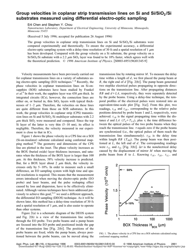
Group velocities in coplanar strip transmission lines on Si and Si/SiO2 /Si substrates measured using differential electro-optic sampling Erli Chen and Stephen Y. Chou Nanostructure Laboratory, Department of Electrical Engineering, University of Minnesota, Minneapolis, Minnesota 55455 ~Received 5 July 1996; accepted for publication 26 August 1996! The group velocities in coplanar strip transmission lines on Si and Si/SiO2/Si substrates were compared experimentally and theoretically. To ensure the experimental accuracy, a differential electro-optic sampling system with a delay-time resolution of 30 fs and a spatial resolution of 1 mm has been developed. Compared with the group velocity on a Si substrate, the group velocity on a Si/SiO2/Si substrate with a 2.2 mm SiO2 layer was found to be 10% faster, which agrees well with the theoretical prediction. © 1996 American Institute of Physics. @S0003-6951~96!01345-9# Velocity measurements have been previously carried out for coplanar transmission lines on a variety of substrates using electro-optic sampling ~EO! techniques.1–8 Recently, the phase velocities in coplanar transmission lines on Si-onsapphire ~SOS! substrates have been studied by Frankel et al.9 In their work, the sapphire layer was 430 mm thick. In integrated circuits ~ICs!, however, the connection lines are either on, or buried in, thin SiO2 layers with typical thicknesses of 1–2 mm. Therefore, the velocities on these lines are quite different from those on SOS substrates. In this work, the group velocities in coplanar strip ~CPS! transmission lines on Si and Si/SiO2 /Si multilayer substrates with 2.2 mm thick SiO2 were measured and compared. Since the top Si layer of the latter is very thin ~5–10 nm!, its effect is negligible. Therefore, the velocity measured in our experiment is close to that in ICs. Figure 1 shows the phase velocity in a CPS line on a SOI ~Si-on-insulator! substrate calculated using conformal mapping method.10 The geometry and dimensions of the CPS line are plotted in the inset. The phase velocity increases as the BOX ~buried oxide! layer thickness increases, and saturates when the thickness of the BOX layer is larger than 100 mm. At this thickness, 58% velocity increase is predicted. But, for a BOX layer about 2 mm thick, the velocity increases only by 5–10%. In order to measure such a small difference, an EO sampling system with high time and spatial resolutions is required. This means that the measurement errors introduced when moving the electro-optic probe ~EO probe! and laser beams, and the pulse reshaping effect caused by loss and dispersion, have to be effectively eliminated. Although various techniques have been addressed previously to achieve this goal,5,11 we used a different approach, the differential EO sampling ~DEOS! technique. As it will be shown later, this method has a delay-time resolution of 30 fs and a spatial resolution of 1 mm, and is also easier to operate than other systems. Figure 2~a! is a schematic diagram of the DEOS system and Fig. 2~b! is a view of the transmission line surface through the EO probe. Two probe beams and a pump beam are focused into the EO probe and positioned inside the gap of the transmission line @Fig. 2~b!#. The positions of the probe beams are fixed, while the pump beam, always positioned between the probe beams, can be moved along the transmission line by rotating mirror M . To measure the delay time within a length of d, we first placed the pump beam at R, the right end of d @Fig. 2~b!#. The pump beam generated two steplike electrical pulses propagating in opposite directions on the transmission line. After propagating distances RB and d1LA, respectively, they were separately detected by the probe beams. Using a delay-line technique, the temporal profiles of the electrical pulses were restored into an equivalent-time-scale plot @Fig. 3~a!#. From this plot, two readings, t 1R and t 2R , corresponding to the relative pulse positions detected by probe beam 1 and 2, respectively, were achieved. t 1R is the signal propagating time within the distance d and LA (T d 1T LA ), plus t, the time difference between the optical pulses of the two probe beams when they reach the transmission line. t equals zero if the probe beams are synchronized ~i.e., the optical pulses of them reach the transmission line simultaneously!. t 2R is the delay time within length RB (T RB ). The pump beam was then positioned at L, the left end of d. The corresponding readings were t 1L and t 2L @Fig. 3~b!#. Dt is the nonelectrical delay caused by the displacement of mirror M when moving the probe beam from R to L. Knowing t 1R , t 2R , t 1L , and FIG. 1. The phase velocity in a CPS line on a SOI substrate calculated using conformal mapping method. Appl. Phys. Lett. 69 (19), 4 November 1996 0003-6951/96/69(19)/2861/3/$10.00 © 1996 American Institute of Physics 2861 Downloaded¬07¬Aug¬2003¬to¬128.112.49.65.¬Redistribution¬subject¬to¬AIP¬license¬or¬copyright,¬see¬http://ojps.aip.org/aplo/aplcr.jsp FIG. 2. ~a! Schematic diagram of the differential EO sampling system. ~b! A view of the transmission line through the EO probe. t 2L , the delay time T d of the line section d can then be calculated as: T d 5 21 @~ t 2L 2t 1L ! 2 ~ t 2R 2t 1R !# . ~1! Referring to Fig. 3, it is not hard to see that all the unwanted delays, t, Dt, T RB , and T LA , are canceled out in Eq. ~1!. In other words, the errors caused by the nonelectrical delay are simply eliminated by a differential technique described in Fig. 2 and Eq. ~1!. The EO probe and the sample stage of the system are fixed during measurements. The two probe beams need not necessarily be synchronized since the asynchronization between the probe beams ~t! is subtracted in Eq. ~1!. Therefore, the two probe beams can be placed anywhere on the transmission line. The above features make a DEOS system simpler and easier to operate than other systems. Most importantly this technique allows us to measure the delay within a very short line length. Thus, the dispersion and absorption from the transmission line and the EO probe are minimized in the measurements, resulting in a very small pulse reshaping effect. However, the delay time measured in this way is different from the actual value since the EO probe affects the signal speed in the transmission line. This loading effect of the probe has to be corrected in order to obtain a correct value. The loading effect can be corrected using the ‘‘loading factor,’’ k, defined as k5 v 0ph v ph , FIG. 3. Diagram for describing the operational procedure of the DEOS system. T d , T LA , and T RB are the delays in the lengths of d, LA, and RB, respectively. t is the time difference between the optical pulses of the probe beams, and Dt is the nonelectrical delay caused by rotating mirror M. conformal mapping method which has considered the multilayer structures of both the transmission line and the probe.10 The structure of the transmission line used for the calculation is indicated in the inset of Fig. 1. The base of each probe is assumed to be 3.7-mm-thick fused silica with a relative dielectric constant of 3.78. In our system, the EO probe has a LiTaO3 crystal with a thickness of 24.0 mm. From Fig. 4, the corresponding loading factor is 2.10. The calculated loading factor for a similar CPS transmission line but on Si substrate is 1.98 ~not shown in Fig. 4!. Both loading factors agree with experimental results within 5%. The spatial resolution of the DEOS system depends on the size of the pump beam, which is determined by the diffraction limit of the microscope used in this system. In the near infrared region, this can be less than 1 mm. The time ~2! where v 0ph is the phase velocity of the transmission without the EO probe and v ph is the phase velocity with the probe. The loading effect is strongly related to the geometry and dimensions of the probe and the transmission line. Figure 4 shows the loading factors of three commonly used probes as a function of the EO crystal’s thickness h, calculated using a FIG. 4. Loading factors of three commonly used EO crystals as a function of their thicknesses. The geometry and dimension of the transmission line used for the calculation is shown in the inset of Fig. 1. 2862 Appl. Phys. Lett., Vol. 69, No. 19, 4 November 1996 E. Chen and S. Y. Chou Downloaded¬07¬Aug¬2003¬to¬128.112.49.65.¬Redistribution¬subject¬to¬AIP¬license¬or¬copyright,¬see¬http://ojps.aip.org/aplo/aplcr.jsp FIG. 5. Delay time vs signal propagating distance for CPS lines on ~a! Si and ~b! SOI substrates. resolution of the system was measured by gradually reducing the line length d until the corresponding delay is undetectable ~i.e., the delay reached the standard error of the system!. The smallest length was found to be approximately 2 mm in our DEOS system, corresponding to a delay time of 30 fs @see Fig. 5~a!#. The dispersion of the system was 0.3 fs/mm. Therefore, the time difference caused by dispersion will be less than the time resolution of the system if the length of the measured transmission line is kept within 100 mm. Under this condition, the measured group velocity is close to the phase velocity in the transmission line. The absorption was 7% in a 200 mm length. The transmission lines were fabricated using photolithography and lift-off techniques. The 30/220-nm-thick Ti/Au conducting strips were 19 mm wide and 10 mm apart. Si/SiO2 /Si substrates were SiBond’s wafer-bonded SOI wafers with a 2.2-mm-thick buried oxide layer. The thickness of the top Si layer was 5–10 nm, which has been thinned by thermal oxidation and HF wet etch. Since the top Si layer is very thin, it has a negligible effect on the velocity. The Si substrate was lightly doped n-type wafer with a thickness of 550 mm. The EO probe used in the system has a 24.0 mm thick LiTaO3 crystal ( e r 543) with a 3.7-mm-thick fused silica base ( e r 53.78). The surface area of the probe is 200 3200 mm2. The probe was in contact with the transmission lines during the measurements. A coherent Ti:sapphire laser with a pulse width of 150 fs was used as the light source. To increase the system’s signal-to-noise ratio, a rf signal mixer was used.12 The rising time and the full width at halfmaximum ~FWHM! of the electrical pulses generated by the pump beam were, respectively, 400 fs and 50 ps for the transmission lines on the Si substrate, and 400 fs and 10 ps for the transmission lines on the SOI substrate. The experimental results are plotted in Fig. 5~a! and 5~b! for CPS lines on Si and SOI, respectively. The plot shows an excellent linearity between the delay time and the propagating distance indicating that the phase velocities in the transmission lines are very close to their quasistatic values. The average group velocities calculated from the experimental data are 1.23 and 1.3631010 cm/s for the CPS lines on Si and on SOI, respectively, with a standard deviation less than 3%. A 10% difference between the two group velocities has been found. Theoretical values calculated using conformal mapping techniques are also plotted in the Figs. 5~a! and 5~b!. The difference between the theoretical and experimental values are less than 5%. In summary, we have demonstrated a differential electro-optic sampling method for measuring the delay time in coplanar transmission lines. A 30 fs delay-time resolution and a 1 mm spatial resolution have been achieved. Using this method, we have found that the group velocity of a CPS transmission line on a SOI substrate with a 2.2-mm-thick buried oxide layer is 10% higher than that on a Si substrate. The experimental results differ only by 5% from the values calculated by a theoretical model achieved using conformal mapping technique. A DEOS system can be used to characterize the imperfections in a transmission line caused by defect, banding, and nonuniformity of the substrate. It can also be used for measuring delay time in ultrafast devices provided that their input and output ends are reversible at small signal conditions. The authors would like to thank SiBond company for supplying the SOI wafer. This work is supported in part by NSF. 1 J. A. Valdmanis, G. Mourou, and C. W. Gabel, Appl. Phys. Lett. 41, 211 ~1982!. 2 K. E. Meyer and G. A. Mourou, in Picosecond Electronics and Optoelectronics, edited by G. A. Mourou, D. M. Bloom, and C. H. Lee ~Springer, New York, 1985!, p. 54. 3 C. J. Kryzak, K. E. Meyer, and G. A. Mourou, in Ref. 2, p. 244. 4 W. H. Knox et al., IEEE J. Quantum Electron. 25, 2586 ~1989!. 5 D. R. Dykaar, A. F. J. Levi, and M. Anzlowar, Appl. Phys. Lett. 57, 1123 ~1990!. 6 H. Roskos, M. C. Nuss, K. W. Goossen, and D. W. Kisker, Appl. Phys. Lett. 58, 2604 ~1991!. 7 U. D. Keil, D. R. Dykaar, A. F. J. Levi, R. F. Kopf, L. N. Pfeiffer, S. B. Darack, and K. W. West, IEEE J. Quantum Electron. 28, 2333 ~1992!. 8 J.-H. Son, H.-H. Wang, J. F. Whitaker, and G. A. Mourou, IEEE Trans Instrum. Meas. 41, 1574 ~1993!. 9 M. Y. Frankel, R. H. Voelker, and J. N. Hilfiker, IEEE Trans. Microwave Theory Tech. 42, 396 ~1994!. 10 E. Chen and S. Y. Chou, IEEE Trans. Microwave Theory Tech. ~submitted!. 11 S. Alexandrou, R. Sobolewski, and T. Y. Hsiang, IEEE J. Quantum Electron. 28, 2325 ~1992!. 12 J. M. Chwalek and D. R. Dykaar, Rev. Sci. Instrum. 61, 1273 ~1990!. Appl. Phys. Lett., Vol. 69, No. 19, 4 November 1996 E. Chen and S. Y. Chou 2863 Downloaded¬07¬Aug¬2003¬to¬128.112.49.65.¬Redistribution¬subject¬to¬AIP¬license¬or¬copyright,¬see¬http://ojps.aip.org/aplo/aplcr.jsp


