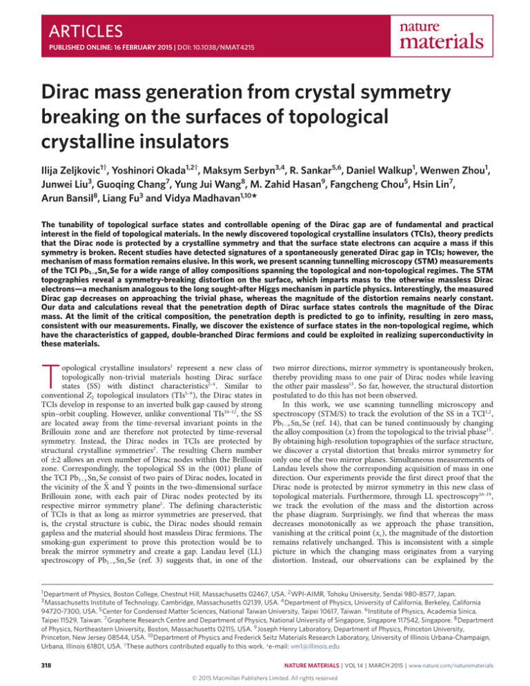
ARTICLES
PUBLISHED ONLINE: 16 FEBRUARY 2015 | DOI: 10.1038/NMAT4215
Dirac mass generation from crystal symmetry
breaking on the surfaces of topological
crystalline insulators
Ilija Zeljkovic1†, Yoshinori Okada1,2†, Maksym Serbyn3,4, R. Sankar5,6, Daniel Walkup1, Wenwen Zhou1,
Junwei Liu3, Guoqing Chang7, Yung Jui Wang8, M. Zahid Hasan9, Fangcheng Chou5, Hsin Lin7,
Arun Bansil8, Liang Fu3 and Vidya Madhavan1,10*
The tunability of topological surface states and controllable opening of the Dirac gap are of fundamental and practical
interest in the field of topological materials. In the newly discovered topological crystalline insulators (TCIs), theory predicts
that the Dirac node is protected by a crystalline symmetry and that the surface state electrons can acquire a mass if this
symmetry is broken. Recent studies have detected signatures of a spontaneously generated Dirac gap in TCIs; however, the
mechanism of mass formation remains elusive. In this work, we present scanning tunnelling microscopy (STM) measurements
of the TCI Pb1−x Snx Se for a wide range of alloy compositions spanning the topological and non-topological regimes. The STM
topographies reveal a symmetry-breaking distortion on the surface, which imparts mass to the otherwise massless Dirac
electrons—a mechanism analogous to the long sought-after Higgs mechanism in particle physics. Interestingly, the measured
Dirac gap decreases on approaching the trivial phase, whereas the magnitude of the distortion remains nearly constant.
Our data and calculations reveal that the penetration depth of Dirac surface states controls the magnitude of the Dirac
mass. At the limit of the critical composition, the penetration depth is predicted to go to infinity, resulting in zero mass,
consistent with our measurements. Finally, we discover the existence of surface states in the non-topological regime, which
have the characteristics of gapped, double-branched Dirac fermions and could be exploited in realizing superconductivity in
these materials.
opological crystalline insulators1 represent a new class of
topologically non-trivial materials hosting Dirac surface
states (SS) with distinct characteristics2–4 . Similar to
conventional Z2 topological insulators (TIs5–9 ), the Dirac states in
TCIs develop in response to an inverted bulk gap caused by strong
spin–orbit coupling. However, unlike conventional TIs10–12 , the SS
are located away from the time-reversal invariant points in the
Brillouin zone and are therefore not protected by time-reversal
symmetry. Instead, the Dirac nodes in TCIs are protected by
structural crystalline symmetries2 . The resulting Chern number
of ±2 allows an even number of Dirac nodes within the Brillouin
zone. Correspondingly, the topological SS in the (001) plane of
the TCI Pb1−x Snx Se consist of two pairs of Dirac nodes, located in
the vicinity of the X̄ and Ȳ points in the two-dimensional surface
Brillouin zone, with each pair of Dirac nodes protected by its
respective mirror symmetry plane1 . The defining characteristic
of TCIs is that as long as mirror symmetries are preserved, that
is, the crystal structure is cubic, the Dirac nodes should remain
gapless and the material should host massless Dirac fermions. The
smoking-gun experiment to prove this protection would be to
break the mirror symmetry and create a gap. Landau level (LL)
spectroscopy of Pb1−x Snx Se (ref. 3) suggests that, in one of the
T
two mirror directions, mirror symmetry is spontaneously broken,
thereby providing mass to one pair of Dirac nodes while leaving
the other pair massless13 . So far, however, the structural distortion
postulated to do this has not been observed.
In this work, we use scanning tunnelling microscopy and
spectroscopy (STM/S) to track the evolution of the SS in a TCI1,2 ,
Pb1−x Snx Se (ref. 14), that can be tuned continuously by changing
the alloy composition (x) from the topological to the trivial phase15 .
By obtaining high-resolution topographies of the surface structure,
we discover a crystal distortion that breaks mirror symmetry for
only one of the two mirror planes. Simultaneous measurements of
Landau levels show the corresponding acquisition of mass in one
direction. Our experiments provide the first direct proof that the
Dirac node is protected by mirror symmetry in this new class of
topological materials. Furthermore, through LL spectroscopy16–19 ,
we track the evolution of the mass and the distortion across
the phase diagram. Surprisingly, we find that whereas the mass
decreases monotonically as we approach the phase transition,
vanishing at the critical point (xc ), the magnitude of the distortion
remains relatively unchanged. This is inconsistent with a simple
picture in which the changing mass originates from a varying
distortion. Instead, our observations can be explained by the
1 Department
of Physics, Boston College, Chestnut Hill, Massachusetts 02467, USA. 2 WPI-AIMR, Tohoku University, Sendai 980-8577, Japan.
Institute of Technology, Cambridge, Massachusetts 02139, USA. 4 Department of Physics, University of California, Berkeley, California
94720-7300, USA. 5 Center for Condensed Matter Sciences, National Taiwan University, Taipei 10617, Taiwan. 6 Institute of Physics, Academia Sinica,
Taipei 11529, Taiwan. 7 Graphene Research Centre and Department of Physics, National University of Singapore, Singapore 117542, Singapore. 8 Department
of Physics, Northeastern University, Boston, Massachusetts 02115, USA. 9 Joseph Henry Laboratory, Department of Physics, Princeton University,
Princeton, New Jersey 08544, USA. 10 Department of Physics and Frederick Seitz Materials Research Laboratory, University of Illinois Urbana-Champaign,
Urbana, Illinois 61801, USA. †These authors contributed equally to this work. *e-mail: vm1@illinois.edu
3 Massachusetts
318
NATURE MATERIALS | VOL 14 | MARCH 2015 | www.nature.com/naturematerials
© 2015 Macmillan Publishers Limited. All rights reserved
NATURE MATERIALS DOI: 10.1038/NMAT4215
300 K
7K
Intensity (a.u.)
200
Se
10
Sn/Pb
111
220
222
311
400 420 422
20 30 40 50 60 70 80
2θ (°)
Figure 1 | Bulk cubic crystal structure of Pb1−x Snx Se. a, Schematic of the
face-centred cubic crystal structure, showing the Se and Pb/Sn sublattices.
b, X-ray diffraction intensity data for x ∼ 0.35, showing a single phase
cubic crystal structure without detectable symmetry breaking as a result
of Sn substitution detected both at room temperature (black) and
7 K (red).
increasing penetration of the SS into the bulk as we approach xc .
In this scenario, the distortion observed in STM is restricted to
the surface. The magnitude of the mass is therefore controlled by
the weight of the SS at the topmost layer, which decreases with
increasing bulk penetration of the SS. Our results thus present direct
experimental evidence in support of the theoretical picture of the
fate of the SS electrons close to the critical composition where the
trivial state is achieved via complete penetration of the bulk of the
sample by the Dirac electrons. Finally, on the trivial side, we make
a surprising discovery of novel remnant SS, which exhibit many of
the characteristics of their topological counterparts.
a
c
Pb1−x Snx Se single crystals in the range of Sn concentrations
studied in this work are expected to have a face-centred cubic structure20 (Fig. 1). From the square atomic lattice seen in the low-bias
STM topographs (Fig. 2c,d), the crystals cleave along the (001) direction, exposing one of the two sublattices. To explore the evolution of
the SS on the (001) face, we perform LL spectroscopy in a magnetic
field on a series of samples spanning the quantum phase transition
from the trivial to the topological phase: x ∼ 0.09 (trivial), 0.17 (critical), 0.29 (topological) and 0.34 (topological) (Fig. 3). Our first task
is to ascertain the existence of Dirac SS in the topological samples.
To accomplish this, we determine the presence of the Dirac nodes
at different Sn concentrations across the transition point (Fig. 3).
The Dirac node signifies the continuous nature of the topological SS
bands, which necessarily span the gap between the conduction and
valance bands. The presence of this topologically protected point
is manifested as a non-dispersing (energy independent of magnetic
field) zeroth LL peak in dI /dV spectra located near the minimum.
We find that such a non-dispersing peak is seen clearly in all three
non-trivial samples (Fig. 3f–h). In contrast, although LLs signifying
the existence of SS are clearly observed even in the trivial x ∼ 0.09
sample (Fig. 3e), the zeroth LL is notably absent, indicating the nontopological nature of the SS.
In the topological samples, we find two additional non-dispersing
peaks, labelled E+∗ and E−∗ (Fig. 3c,d,g,h) on either side of the
zeroth LL peak. The non-dispersing nature and the coexistence of
the E ∗ peaks with the peak at the Dirac point suggest that the
E ∗ peaks correspond to mass acquisition in two out of the four
Dirac cones within the first Brillouin zone (Fig. 4a)3 . The resulting
mass energy scale can be characterized by the mass gap ∆ = |E+∗ −
E−∗ |. Interestingly, we find that ∆ decreases monotonically from
∼24.2 meV for x ∼ 0.38 to ∼0 meV near the critical doping of
e
g
i
|Re| part of FFT (a.u.)
b
Se
0.5
0.0
Pb
Se
−0.5
−0.5 0.0 0.5 1.0 1.5
X coordinate (fraction of a0)
Qx
3 nm
Low
0
j
h
f
both sublattices
1.0
Qx
Qy
0.95 1.00 1.05
Fraction of |Qmag|
−400 mV
Both sublattices
Y coordinate (fraction of a0)
d
1.5
Pb
Qy
3 nm
[110] [110] a = 3.05 Å
0
b
Qx
one sublattice
One sublattice
−100 mV
High
Negative
Positive
Qy
|Im| part of FFT (a.u.)
a
ARTICLES
Qx
Qy
0
0.95 1.00 1.05
Fraction of |Qmag|
Figure 2 | Symmetry-breaking distortion on the surface of Pb1−x Snx Se. a, Schematic representation of the distortion in the surface layer. Two sublattices
shift in opposite manners along the [110] direction, as denoted by red arrows. Even though [110] mirror symmetry is still preserved (green line), the
distortion breaks [110] mirror symmetry (dashed red line). Dashed black circles represent the ideal atomic positions in a cubic lattice without the
distortion. b, Average 2 × 2-atom supercell obtained from the experimental topograph in d. The centres of average atoms determined by Gaussian fitting
are denoted by yellow and orange dots, and the dashed square represents the tetragonal unit cell in the absence of distortion (see Supplementary
Discussion I for more details). c,d, STM topographs of the x ∼ 0.38 sample showing only the Se sublattice (c; see Supplementary Discussion II) and both
sublattices (d) acquired over the same area of the sample. Insets in c,d show a 4 × 4-atom supercell aligned along the atomic Bragg peak directions24 .
Yellow and orange dots represent the centres of Se and Pb/Sn atoms, respectively. e,f, Real part of the Fourier transform of the STM topographs in c,d,
respectively. g,h, Imaginary part of the Fourier transform of STM topographs in c,d, respectively. i, Line cut starting from the centre of the Fourier transform
in e through the atomic Bragg peaks Qx and Qy , showing the C4 symmetry of our STM tip. j, Line cut starting from the centre of the Fourier transform in h
through the atomic Bragg peaks Qx and Qy , showing the symmetry-breaking distortion present along only the Qy direction. STM set-up conditions are:
Iset = 200 pA, Vset = −100 mV (c); Iset = 900 pA, Vset = −400 mV (d).
NATURE MATERIALS | VOL 14 | MARCH 2015 | www.nature.com/naturematerials
© 2015 Macmillan Publishers Limited. All rights reserved
319
NATURE MATERIALS DOI: 10.1038/NMAT4215
ARTICLES
Topological phase transition
Trivial
7.5 T
x ∼ 0.09
Critical
b
Topological
c
x ∼ 0.17
7.5 T
7.5 T
0T
Dirac point
No Dirac point
0T
−2 −2 −1
−3 −1
1 2 1 2 34 5
67
f
7.5 T−4−3 −2−1
0 1
2 34
5 6 78
g
Dirac point
x ∼ 0.34
7.5 T Dirac point
E−∗ E∗
+
EVHS+
−1
0
1
3
4
5
6
h
7 89
7.5 T−2 −1
7.0 T
7.0 T
7.0 T
6.5 T
6.5 T
6.5 T
6.5 T
6.0 T
6.0 T
6.0 T
6.0 T
5.5 T
5.5 T
5.5 T
5.5 T
5.0 T
5.0 T
5.0 T
4.5 T
4.5 T
4.5 T
4.5 T
3.0 T
3.0 T
3.0 T
3.0 T
−200
−100
0
Bias voltage (mV)
−150 −100 −50
0
50
Bias voltage (mV)
−100
−50
0
Bias voltage (mV)
50
EVHS+
EVHS−
7.0 T
5.0 T
E∗+
E−∗
0T
EVHS−
7.5 T
Topological
d
x ∼ 0.29
0T
7.5 T
Background subtracted dI/dV (a.u.)
e
Raw dI/dV (a.u.)
a
0
1
9 11 1314
10
12 15
−150 −100
−50
0
Bias voltage (mV)
Figure 3 | Landau level spectroscopy. a–d, Average dI/dV curves acquired at magnetic fields of 0 T and 7.5 T over the same area of the sample for Sn
fractions x ∼ 0.09, 0.17, 0.29 and 0.34 Sn, respectively. e–h, Waterfall plots of background subtracted dI/dV curves (see Supplementary Discussion III for
normalization details) acquired as a function of magnetic field, showing LLs as prominent dispersing ripples. Indexing of LLs used to plot the dispersions in
Fig. 6 is denoted in each panel. No Dirac point is present in the trivial sample (e), whereas a prominent non-dispersing peak that develops under application
∗ and E ∗ , indicate the presence of massive
of a magnetic field signals the Dirac node formation in f–h. Other non-dispersing peaks in c,d,g,h, labelled as E+
−
3
Dirac fermions . EVHS+ and EVHS− denote the positions of two van Hove singularities, which are directly related to the two Lifshitz transitions. STM set-up
conditions are: Iset = 300 pA, Vset = −200 mV (a); Iset = 385 pA, Vset = 70 mV (b); Iset = 540 pA, Vset = 50 mV (c); Iset = 350 pA, Vset = 50 mV (d).
x ∼ 0.17 (Fig. 4c). To establish the mechanism of the mass formation
and to understand its variation across the phase diagram, the next
step is to image any mirror-symmetry-breaking distortion present
in our samples.
In principle, STM images should be able to detect structural
deformations. However, conventional low-bias topographs (Fig. 2c)
showed only one of the two (either Pb/Sn or Se) sublattices,
which is a square lattice with no detectable distortion3 . In the
present study, by systematically adjusting the imaging conditions21 ,
we were able to detect both sublattices (Fig. 2d). We note here
that, because STM measures the local density of states as well as
the atomic corrugations22 , one cannot always attribute periodic
structures in STM topographies to atomic positions. In our case,
by careful measurements of a series of bias-dependent topographies
in multiple alloys of Pb1−x Snx Se, we were able to establish that
the low-bias topography shows the Se atoms whereas the higherbias topographies show the Pb/Sn as well as the Se lattices (see
Supplementary Discussion I for more details).
We now have sufficient information to look for signs of a mirrorsymmetry-breaking distortion. Even though the higher-bias images
exhibit a range of contrasts, we find that a distortion of the square
lattice can be observed in local patches by eye. However, to explain
the mass acquisition, we have to determine whether a long-range
phase-coherent distortion exists in our sample. To establish this
we create an average 4 × 4-atom ‘supercell’23,24 (inset in Fig. 2c,d).
The average unit cell clearly reveals a relative in-plane atomic shift
between the two sublattices (Fig. 2a), resulting in a characteristic
zigzag pattern (see Supplementary Discussion I for more details).
This suggests that there is a single dominant domain within our
field of view. This distortion, also known to occur within the bulk
320
of the endmember SnSe (ref. 25), breaks one of the two [110] mirror
symmetries (Fig. 2a,b), leaving the other symmetry unaffected. To
further substantiate the symmetry breaking observed in real space,
we examine the two-dimensional Fourier transforms (FTs) of the
STM topographs (Fig. 2e–j). The distortion observed should result
in an effective broken C4 symmetry when both sublattices are
observed. We find that when only one sublattice is imaged at lower
biases, the real parts of the Fourier components at the atomic Bragg
peak wavevectors Qx and Qy have the same magnitude (Fig. 2e,i),
whereas the respective imaginary parts are negligible (Fig. 2g),
both consistent with the observed square lattice. We note that this
also demonstrates the symmetry of our STM tip. Next, in STM
topographs showing both sublattices acquired using the same STM
tip, we find that an imaginary component emerges along exclusively
one lattice direction (Qy , but not Qx ). This corresponds to the
C4 symmetry breaking in the sample crystal structure (Fig. 2h,j),
further confirming the long-range nature of the distortion. Our
results present the first direct evidence for the generation of massive
Dirac fermions out of the pool of their massless counterparts due to
spontaneously broken crystal symmetry.
Next, we measure the magnitude of the distortion as a function
of alloy composition. This would help us determine whether the
decrease in the mass gap as we approach the critical concentration
arises simply from a decrease in the magnitude of the observed
distortion. Surprisingly we find that the magnitude of the structural
distortion does not change significantly across the phase diagram
(Fig. 4d), which implies that the mass variation occurs as a result
of a different process. Our data suggest an alternative explanation
for the Dirac gap variation, based on two factors: the broken crystal
symmetry is present exclusively on the surface, and the surface state
NATURE MATERIALS | VOL 14 | MARCH 2015 | www.nature.com/naturematerials
© 2015 Macmillan Publishers Limited. All rights reserved
NATURE MATERIALS DOI: 10.1038/NMAT4215
ARTICLES
b
a
E−∗
Dirac point
E∗+
Γ
X
Y
Δ
dI/dV (a.u.)
x ∼ 0.29
x ∼ 0.34
M
x ∼ 0.38
−20
+20
0
Energy offset from Dirac point (meV)
c
d
30
e
0.4
0.08
Δ (meV)
20
15
10
5
0.3
Weight of the surface layer (%)
Distortion magnitude (fraction of a0)
25
0.2
0.1
0.06
0.04
0.02
0
0.0
0.0
0.1
0.2
0.3
0.4
Sn composition x
0.5
0.00
0.0
0.1
0.2 0.3 0.4
Sn composition x
0.5
0.0
0.1
0.2 0.3 0.4
Sn composition x
0.5
Figure 4 | Evolution of the Dirac gap with alloy composition. a, Illustration of the Dirac gap ∆ opening in two out of the four Dirac cones within the first
Brillouin zone owing to a broken [1̄10] mirror plane. b, Composition dependence of average dI/dV spectra acquired at 7.5 T, showing the evolution of the
non-dispersing E∗ LL peaks. c, Plot of ∆ versus Sn composition, showing a monotonic increase in ∆ in the topological regime. d, Magnitude of the distortion
as a function of Sn composition, showing the presence of distortion of similar magnitude across a wide range of compositions (see Supplementary
Discussion IV for more details). e, Theoretical calculations of the surface layer contribution to the Dirac wavefunction, showing a monotonic increase
(penetration depth effectively decreases) with increased Sn doping. Orange lines in c-e represent guides for the eye. The width of the orange lines are for
visualization purposes only. Vertical error bars in c,d are explained in Supplementary Discussions III and V, respectively.
penetration depth λSS increases on approaching xc . In this scenario,
the fraction of Dirac electrons sampling the broken-symmetry
region decreases on approaching xc , effectively ‘washing out’ the
effect of the surface symmetry breaking, and thus creating a smaller
Dirac mass.
To determine the validity of the scenario, we first determine
whether the bulk is distorted. Our X-ray measurements in fact show
a temperature-independent, bulk cubic structure, supporting the
idea that the cubic symmetry is broken only at the surface (Fig. 1b).
Let us now consider the second factor. According to theory, the
weight of Dirac SS at the surface of a topological insulator is not
a constant. An estimate for the length scale of the surface modes in
the z-direction (perpendicular to the surface) is λSS = h̄v/Eg , where
v is the velocity of the Dirac fermions and Eg is the energy gap of
the bulk states26 . This implies that if one could continuously tune
the bulk bandgap, as the magnitude of the gap shrinks, the Dirac
SS would penetrate progressively further into the bulk, ultimately
penetrating the entire sample at the critical point when the bulk
gap closes. To quantitatively determine the surface weight of the
SS as a function of composition, we use band structure parameters
from our tight-binding model with varying Sn composition and
calculate the percentage of the SS wavefunction in the topmost layer
(Fig. 4e). Our calculations reveal that the SS weight on the top layer
indeed decreases monotonically on approaching xc , reflecting the
penetration depth going to infinity near the quantum critical point.
This, coupled with a distortion confined to the surface layers, is
sufficient to explain our experimentally observed trend in the mass
gap. In contrast, if we assume that the distortion persists within the
bulk of the material, our calculations indicate that the gap would be
nearly constant as a function of alloying content, which contradicts
our experimental observations (Supplementary Information VI).
Our experiments therefore indicate that the magnitude of the mass
in our samples is controlled by the SS penetration into the bulk.
Remarkably, our data represent the first observation of the striking
effects of the divergent SS penetration depth on topological SS as the
bulk approaches the critical concentration.
NATURE MATERIALS | VOL 14 | MARCH 2015 | www.nature.com/naturematerials
© 2015 Macmillan Publishers Limited. All rights reserved
321
NATURE MATERIALS DOI: 10.1038/NMAT4215
ARTICLES
a
b
Topological
CB
CB
Upper
Dirac cone
SS
?
SS
Lower
Dirac cone
VB
2|E+∗ − E−∗|
|EVHS+ − EVHS−|/2
vf
8
vf ( 105 m s−1)
Energy
CB
60
10
xc
30
4
20
2
Trivial
regime
0
0.0
Doping
40
6
VB
VB
50
10
Topological
regime
0.1
0.2
Sn composition
0.3
0
|EVHS+ − EVHS−|/2, 2|E+∗ − E−∗| (meV)
Trivial
0.4
Figure 5 | Evolution of band structure with alloy composition. a, Schematic phase diagram of TCIs. The bandgap between the conduction (CB) and valence
bands (VB) closes at a critical Sn concentration xc of approximately 0.18 (ref. 14), causing band inversion and the formation of topologically protected SS
consisting of two Dirac cones centred at each X̄ and Ȳ point. The question mark denotes one of the unknowns in the field regarding what surface states, if
any, appear on the trivial side, and how they relate to their topological counterparts. b, Evolution of band structure parameters as a function of Sn
composition. Average SS dispersion velocity v̄f assuming isotropic momentum dispersion, 2∆ and the energy of the Lifshitz transition are shown as green
squares, yellow circles and blue triangles, respectively. Horizontal error bars denote the standard deviation in EDS measurements of Sn composition from
five different areas of each sample. Vertical error bars are explained in Supplementary Discussion III.
a
b
x ∼ 0.09
0
0
d
x ∼ 0.29
x ∼ 0.34
0
−100
−50
Bias voltage (mV)
−50
Bias voltage (mV)
0
Bias voltage (mV)
Bias voltage (mV)
c
x ∼ 0.17
−50
n
−50
15
10
5
0
−5
−100
−150
−100
−100
−10
−5
0
5
10
−10
sgn(n)∗(nB)1/2
e
−5
0
5
10
f
X
−10
sgn(n)∗(nB)1/2
−5
0
5
sgn(n)∗(nB)1/2
−10
0
−5
5
sgn(n)∗(nB)1/2
10
h
g
X
10
X
X
Figure 6 | Evolution of SS across the topological quantum phase transition. a–d, Plots of LL dispersion before (a), at (b) and after (c,d) the topological
transition. The double-branch dispersion in a shows the proximity state without the Dirac node, which is clearly observed in topological samples in b–d.
Two Dirac cones are nearly indistinguishable in b, but become increasingly offset in energy with increasing Sn content (c,d). Non-dispersing E∗ peaks in c,d
(white circles), are absent in the transition sample in b, which allows us to visualize the effect of composition changes on the Dirac gap, a property directly
related to the Dirac fermion mass. Orange lines in a–d schematically depict the low-energy SS dispersions. Grey shaded regions indicate the positions of
the bulk bands determined from ref. 14. Fits to the k · p model34 are shown in Supplementary Discussion V. e–h, Illustrations of the SS band structure
around the X̄ point in the absence of symmetry-breaking surface distortion, showing its evolution from the trivial to the topological regime. The absence of
∗ and E ∗ peaks at the transition point x ∼ 0.17 (Fig. 3b) suggests that ∆ is approximately zero at this concentration.
separate E+
−
Having understood the mechanism of mass acquisition, we
turn to the evolution of the dispersion of SS across the critical
composition, schematically portrayed in Fig. 5a. To extract the
dispersion of the SS bands, we first need to index field-dispersing
322
LLs and plot them as a function of (nB)0.5 . As previously
demonstrated3 , this can be a non-trivial process owing to the
complex band structure of topological SS involving multiple Dirac
cones, which hybridize and go through a Lifshitz transition.
NATURE MATERIALS | VOL 14 | MARCH 2015 | www.nature.com/naturematerials
© 2015 Macmillan Publishers Limited. All rights reserved
NATURE MATERIALS DOI: 10.1038/NMAT4215
We determine the LL indices by using the (nB)0.5 scaling behaviour
to collapse the dispersion onto a continuous line. At the Lifshitz
transition, the area of the constant energy contour changes rapidly,
resulting in the van Hove singularities (VHS) observed in our
dI /dV spectra (Fig. 3c,d) and a ‘jump’ in the LL indices13 (for
example in Fig. 3g, the LL index jumps from n = 1 to n = 3). We begin
with the LL plot of the topological sample at x ∼ 0.34 (Fig. 6d), which
reveals many of the features of the SS band structure, including the
Lifshitz transitions schematically shown in Fig. 6h. In a sample with
a lower Sn concentration (x ∼ 0.29; Fig. 6c), we find that both the
Dirac points of the upper and lower Dirac cones and VHS within
each pair move closer to each other in energy than those in the
x ∼ 0.34 sample (Figs 5b and 6g), consistent with previous angleresolved photoemission spectroscopy (ARPES) studies on a closely
related TCI family27,28 . Following this trend, in the sample close to
the transition point (x ∼ 0.17), the SS almost completely overlap
each other (within our resolution, we see only one), as schematically
depicted in Fig. 5a. At this critical concentration, the V-shape of the
dI /dV spectrum near the Dirac point disappears. Because the Vshape reflects the pure SS density of states far from the bulk bands,
its absence suggests that the bulk gap at this concentration is close
to zero, consistent with the critical point.
Finally, we turn our attention to the SS observed in the trivial
phase below xc (Fig. 3a,e). Using the same method of scaling
as used for indexing the LLs of topological samples (Fig. 6b–d),
we obtain a double-branched dispersion for both positive and
negative LLs (Fig. 6a). Owing to the absence of a Dirac point
and the double-branch dispersion, one might simply attribute
these SS to conventional Rashba-split states, most notably known
to occur on metal surfaces. However, the characteristics of the
observed SS differ substantially from conventional Rashba states
and should instead be viewed as topology-induced proximity
states. In contrast to trivial surface states in metals, such as those
occurring on Cu(111) or Au(111), which have two quadratic
dispersions shifted in momentum space29,30 , both branches of
our proximity SS exhibit linear dispersion away from the band
bottom (coefficient of determination R2 for the linear regression
of all branches ∼0.99) (Fig. 6a), with the dispersion velocity
being constant (within ∼7%) in all samples (Fig. 5b). This
indicates an intimate connection between SS in the topological and
non-topological regimes.
These observations strongly suggest that the persistent SS in
trivial TCIs are remnants of the nearby topological phase, rather
than a simple consequence of the boundary conditions at the
surface. Physically, the trivial SS can be understood in the following
way. Like the topological SS, we start with two Dirac cones at
the X point; however, when the bulk transitions into the trivial
regime, the character of the SS changes such that mirror symmetry
no longer protects the intersecting SS from being fully gapped
out, leading to the trivial states shown in Fig. 6e. We note that
the splitting of the two branches is ∼0.01 Å−1 , which is at the
border of momentum resolution of state-of-the-art laser ARPES
studies, and could explain the inability to observe similar SS
splitting31,32 . Our findings open up a new venue for characterizing
and engineering highly tunable two-dimensional electron gases with
novel properties. The highly symmetric nature and linear dispersion
of the proximity SS bands and the large gap could potentially be
exploited in constructing a new generation of electronics, based on
Dirac SS. Furthermore, the geometric shape of these states inevitably
creates a large density of states at the SS band edge, which could
be used in realizing superconductivity in these systems if the Fermi
level is tuned close to this energy by electrostatic gating33 . Finally,
the topological SS that harbour both massive and massless Dirac
fermions present a unique platform for future applications, as they
can be independently tuned via structural symmetry breaking and
alloying composition.
ARTICLES
Methods
Pb1−x Snx Se single crystals with various Sn concentrations were grown by a
self-selecting vapour growth method, cleaved in ultrahigh vacuum at 77 K, and
immediately inserted into the STM head, where they are held at 4 K. We
determine the composition by performing energy-dispersive X-ray spectroscopy
(EDS) on multiple spots on each sample and averaging the obtained values.
Received 18 July 2014; accepted 8 January 2015;
published online 16 February 2015
References
1. Fu, L. Topological crystalline insulators. Phys. Rev. Lett. 106, 106802 (2011).
2. Hsieh, T. H. et al. Topological crystalline insulators in the SnTe material class.
Nature Commun. 3, 982 (2012).
3. Okada, Y. et al. Observation of Dirac node formation and mass acquisition in a
topological crystalline insulator. Science 341, 1496–1499 (2013).
4. Zeljkovic, I. et al. Mapping the unconventional orbital texture in topological
crystalline insulators. Nature Phys. 10, 572–577 (2014).
5. Hsieh, D. et al. A topological Dirac insulator in a quantum spin Hall phase.
Nature 452, 970–974 (2008).
6. Xia, Y. et al. Observation of a large-gap topological-insulator class with a single
Dirac cone on the surface. Nature Phys. 5, 398–402 (2009).
7. Chen, Y. L. et al. Experimental realization of a three-dimensional topological
insulator, Bi2 Te3 . Science 325, 178–181 (2009).
8. Hsieh, D. et al. A tunable topological insulator in the spin helical Dirac
transport regime. Nature 460, 1101–1105 (2009).
9. Roushan, P. et al. Topological surface states protected from backscattering by
chiral spin texture. Nature 460, 1106–1109 (2009).
10. Fu, L., Kane, C. & Mele, E. Topological insulators in three dimensions. Phys.
Rev. Lett. 98, 106803 (2007).
11. Qi, X-L. & Zhang, S-C. Topological insulators and superconductors. Rev. Mod.
Phys. 83, 1057–1110 (2011).
12. Hasan, M. Z. & Kane, C. L. Colloquium: Topological insulators. Rev. Mod. Phys.
82, 3045–3067 (2010).
13. Serbyn, M. & Fu, L. Symmetry breaking and Landau quantization in
topological crystalline insulators. Phys. Rev. B 90, 035402 (2014).
14. Dziawa, P. et al. Topological crystalline insulator states in Pb1−x Snx Se. Nature
Mater. 11, 1023–1027 (2012).
15. Xu, S-Y. et al. Observation of a topological crystalline insulator phase and
topological phase transition in Pb1−x Snx Te. Nature Commun. 3, 1192 (2012).
16. Hashimoto, K. et al. Quantum Hall transition in real space: From localized to
extended states. Phys. Rev. Lett. 101, 256802 (2008).
17. Li, G. & Andrei, E. Y. Observation of Landau levels of Dirac fermions in
graphite. Nature Phys. 3, 623–627 (2007).
18. Hanaguri, T., Igarashi, K., Kawamura, M., Takagi, H. & Sasagawa, T.
Momentum-resolved Landau-level spectroscopy of Dirac surface state in
Bi2 Se3 . Phys. Rev. B 82, 081305 (2010).
19. Soumyanarayanan, A. et al. Imaging the nanoscale band structure of
topological Sb. Preprint at http://arxiv.org/abs/1311.1758 (2013).
20. Agnihotri, O. P., Jain, A. K. & Gupta, B. K. X-ray investigations on
Bridgeman-grown Pb1−x Snx Te single crystals. Mater. Sci. Eng. 38,
33–34 (1979).
21. Gyenis, A. et al. Quasiparticle interference on the surface of the topological
crystalline insulator Pb1−x Snx Se. Phys. Rev. B 88, 125414 (2013).
22. Klijn, J. et al. STM measurements on the InAs(110) surface directly
compared with surface electronic structure calculations. Phys. Rev. B 68,
205327 (2003).
23. Lawler, M. J. et al. Intra-unit-cell electronic nematicity of the high-Tc
copper-oxide pseudogap states. Nature 466, 347–351 (2010).
24. Zeljkovic, I. et al. Scanning tunnelling microscopy imaging of
symmetry-breaking structural distortion in the bismuth-based cuprate
superconductors. Nature Mater. 11, 585–589 (2012).
25. Snykers, M., Delavignette, P. & Amelinckx, S. The domain structure of GeTe as
observed by electron microscopy. Mater. Res. Bull. 7, 831–839 (1972).
26. Linder, J., Yokoyama, T. & Sudbø, A. Anomalous finite size effects on surface
states in the topological insulator Bi2 Se3 . Phys. Rev. B 80, 205401 (2009).
27. Tanaka, Y. et al. Experimental realization of a topological crystalline insulator
in SnTe. Nature Phys. 8, 800–803 (2012).
28. Tanaka, Y. et al. Tunability of the k-space location of the Dirac cones in the
topological crystalline insulator Pb1−x Snx Te. Phys. Rev. B 87, 155105 (2013).
29. Hoesch, M. et al. Spin structure of the Shockley surface state on Au(111). Phys.
Rev. B 69, 241401 (2004).
30. LaShell, S., McDougall, B. & Jensen, E. Spin splitting of an Au(111) surface state
band observed with angle resolved photoelectron spectroscopy. Phys. Rev. Lett.
77, 3419–3422 (1996).
NATURE MATERIALS | VOL 14 | MARCH 2015 | www.nature.com/naturematerials
© 2015 Macmillan Publishers Limited. All rights reserved
323
NATURE MATERIALS DOI: 10.1038/NMAT4215
ARTICLES
31. Wojek, B. et al. Spin-polarized (001) surface states of the topological crystalline
insulator Pb0.73 Sn0.27 Se. Phys. Rev. B 87, 115106 (2013).
32. Yan, C. et al. Experimental observation of Dirac-like surface states and
topological phase transition in Pb1−x Snx Te(111) films. Phys. Rev. Lett. 112,
186801 (2014).
33. Goldstein, G., Aron, C. & Chamon, C. Band-edge superconductivity. Preprint
at http://arxiv.org/abs/1410:6103 (2014).
34. Liu, J., Duan, W. & Fu, L. Two types of surface states in topological crystalline
insulators. Phys. Rev. B 88, 241303 (2013).
Acknowledgements
We thank R. Buczko, C. Chamon, J. C. Seamus Davis, M. El-Batanouny, A. Mesaros,
Y. Ran and A. Soumyanarayanan for useful conversations and G. McMahon for help with
EDS measurements. V.M. gratefully acknowledges funding from the US Department of
Energy, Scanned Probe Division under Award Number DE-FG02-12ER46880 for the
support of I.Z., Y.O., W.Z. and D.W. for this project. Work at Massachusetts Institute of
Technology is supported by US Department of Energy, Office of Basic Energy Sciences,
Division of Materials Sciences and Engineering under Award DE-SC0010526 (L.F.), and
NSF-DMR-1104498 (M.S.). H.L. acknowledges the Singapore National Research
Foundation for support under NRF Award No. NRF-NRFF2013-03. Y.O. was partly
supported by JSPS KAKENHI Grant Numbers 26707016 and 00707656. The work at
Northeastern University is supported by the US Department of Energy grant number
DE-FG02-07ER46352, and benefited from Northeastern University’s Advanced Scientific
324
Computation Center (ASCC), theory support at the Advanced Light Source, Berkeley
and the allocation of supercomputer time at the NERSC through DOE grant number
DE-AC02-05CH11231. Work at Princeton University is supported by the US National
Science Foundation Grant, NSF-DMR-1006492. F.C. acknowledges the support provided
by MOST-Taiwan under project number NSC-102-2119-M-002-004.
Author contributions
Y.O. and I.Z. contributed equally to this work. Y.O., I.Z. and V.M. designed the
experiments. STM experiments were carried out by Y.O., I.Z., D.W. and W.Z. I.Z., Y.O.,
L.F. and V.M. analysed the data and wrote the paper. Samples were obtained from R.S.,
F.C. and M.Z.H. F.C. and R.S. contributed to the single-crystal growth and structural
analysis. L.F. conceived the theoretical explanation for this work. M.S. performed
analytical model calculations. H.L. and A.B. supervised the first-principles part of the
work, which was performed by G.C., Y.J.W., J.L. and H.L.
Additional information
Supplementary information is available in the online version of the paper. Reprints and
permissions information is available online at www.nature.com/reprints.
Correspondence and requests for materials should be addressed to V.M.
Competing financial interests
The authors declare no competing financial interests.
NATURE MATERIALS | VOL 14 | MARCH 2015 | www.nature.com/naturematerials
© 2015 Macmillan Publishers Limited. All rights reserved
