OA-27 Low-Sensitivity, Lowpass Filter Design
advertisement
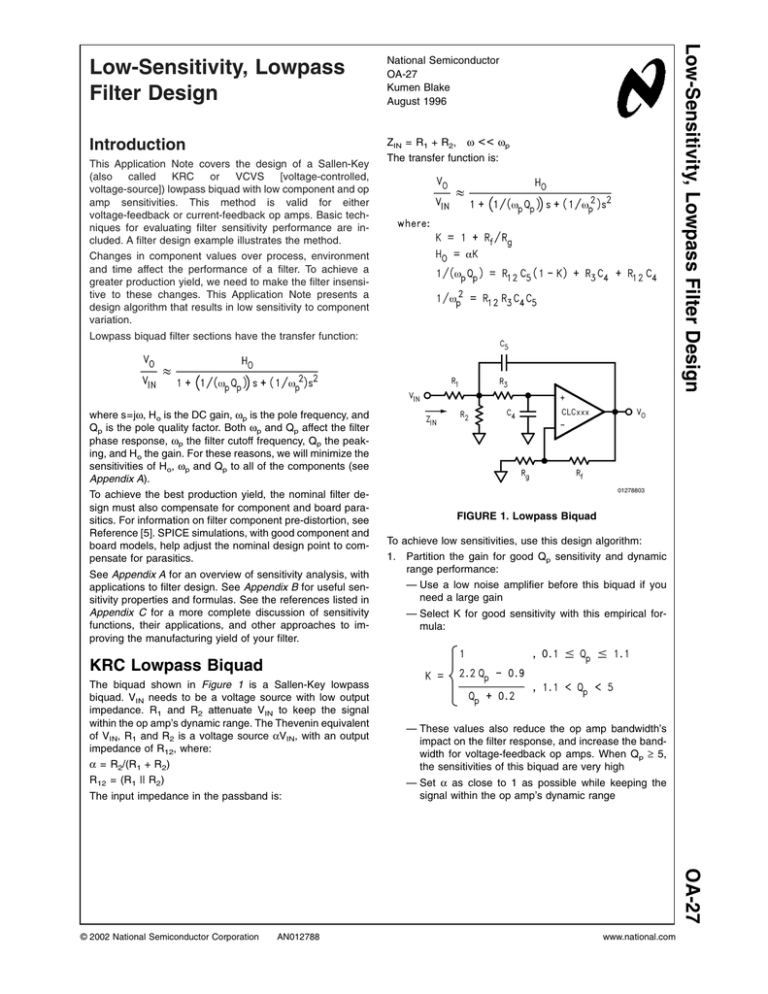
National Semiconductor OA-27 Kumen Blake August 1996 Introduction ZIN = R1 + R2, ω << ωp The transfer function is: This Application Note covers the design of a Sallen-Key (also called KRC or VCVS [voltage-controlled, voltage-source]) lowpass biquad with low component and op amp sensitivities. This method is valid for either voltage-feedback or current-feedback op amps. Basic techniques for evaluating filter sensitivity performance are included. A filter design example illustrates the method. Low-Sensitivity, Lowpass Filter Design Low-Sensitivity, Lowpass Filter Design Changes in component values over process, environment and time affect the performance of a filter. To achieve a greater production yield, we need to make the filter insensitive to these changes. This Application Note presents a design algorithm that results in low sensitivity to component variation. Lowpass biquad filter sections have the transfer function: where s=jω, Ho is the DC gain, ωp is the pole frequency, and Qp is the pole quality factor. Both ωp and Qp affect the filter phase response, ωp the filter cutoff frequency, Qp the peaking, and Ho the gain. For these reasons, we will minimize the sensitivities of Ho, ωp and Qp to all of the components (see Appendix A). To achieve the best production yield, the nominal filter design must also compensate for component and board parasitics. For information on filter component pre-distortion, see Reference [5]. SPICE simulations, with good component and board models, help adjust the nominal design point to compensate for parasitics. See Appendix A for an overview of sensitivity analysis, with applications to filter design. See Appendix B for useful sensitivity properties and formulas. See the references listed in Appendix C for a more complete discussion of sensitivity functions, their applications, and other approaches to improving the manufacturing yield of your filter. 01278803 FIGURE 1. Lowpass Biquad To achieve low sensitivities, use this design algorithm: 1. Partition the gain for good Qp sensitivity and dynamic range performance: — Use a low noise amplifier before this biquad if you need a large gain — Select K for good sensitivity with this empirical formula: KRC Lowpass Biquad The biquad shown in Figure 1 is a Sallen-Key lowpass biquad. VIN needs to be a voltage source with low output impedance. R1 and R2 attenuate VIN to keep the signal within the op amp’s dynamic range. The Thevenin equivalent of VIN, R1 and R2 is a voltage source αVIN, with an output impedance of R12, where: α = R2/(R1 + R2) R12 = (R1 || R2) The input impedance in the passband is: — These values also reduce the op amp bandwidth’s impact on the filter response, and increase the bandwidth for voltage-feedback op amps. When Qp ≥ 5, the sensitivities of this biquad are very high — Set α as close to 1 as possible while keeping the signal within the op amp’s dynamic range OA-27 © 2002 National Semiconductor Corporation AN012788 www.national.com OA-27 KRC Lowpass Biquad • (Continued) 2. Select an op amp with adequate bandwidth (f3 dB) and slew rate: (SR): f3 dB ≥ 10fc SR > 5fc Vpeak where fc is the corner frequency of the filter, and Vpeak is the largest peak voltage. Make sure the op amp is stable at a gain of Av = K. 3. Select Rf and Rg so that: K = 1 + Rf/Rg Select R1 and R2 to properly terminate the transmission line (R1 includes the source resistance) Calculate α and R12 Adjust C and R so that R12 = rR • • To evaluate the sensitivity performance of this design, follow these steps: 1. Calculate the resulting sensitivities: For current-feedback op amps, use the recommended value of Rf for a gain of Av = K. For voltage-feedback op amps, select Rf for noise and distortion performance. This Initialize the resistance level value is a compromise between noise performance, distortion performance, and adequate isolation between the op amp outputs and the capacitors. the resis5. Initialize the capacitance level tor ratio (r2 = R12 / R3), the capacitor ratio (c2 = C4/C5) and the capacitors: C = 1/(Rωp) r2 = 0.10 4. C4 = cC C5 = C/c Set the capacitors C4 and C5 to the nearest standard values. 7. Recalculate C, c2, R and r2: 6. Reducing lowers the biquad’s sensitivity to the op amp bandwidth. c2 = C4/C5 R = 1/(Cωp) 8. Calculate R12 and the resistors: R12 = rR R1 = R12/α R2 = R12/(1–α) R3 = R/r VIN can represent a source driving a transmission line, with R1 and R2 the source and terminating resistances. For this type of application, make these modifications to the design algorithm: www.national.com 2 2. The nominal filter specifications are: (Continued) fc = 500 MHz (passband edge frequency) fs = 100 MHz (stopband edge frequency) Ap = 0.5 dB (maximum passband ripple) As = 19 dB (minimum stopband attenuation) Ho = 0 dB (DC voltage gain) Calculate the relative standard deviations of Ho, ωp and Q p: The 3rd-order Chebyshev filter meets our specifications (see References [1–4]). The resulting −3 dB frequency is 58.4 MHz. The pole frequencies and quality factors are: In this formula, use: — The nominal values of Ho, ωp and Qp for X — The nominal values of R1, R2, R3, Rf, Rg, C4 and C5 for αi (do not use K since it is not a component) — The capacitor and resistor standard deviations for σαi. For parts with a uniform probability distribution, 3. OA-27 KRC Lowpass Biquad Section ωp/2π Qp [MHz] [ ] A B 53:45 31:30 1.706 — Overall Design: 1. Restrict the resistor and capacitor ratios to: 0.1 ≤ r2 ≤ 10 0.1 ≤ c2 ≤ 10 2. Use 1% resistors (chip metal film, 1206 SMD, 25 ppm/˚C) 3. Use 1% capacitors (ceramic chip, 1206 SMD, 100 ppm/˚C) 4. Use standard resistor and capacitor values 5. The temperature range is −40˚C to 85˚C, and room temperature is 25˚C Section A Design: 1. Use the CLC111. This is a closed-loop buffer. — f3 db = 800 MHz > 10 fc = 500 MHz — SR = 3500V/µs, while a 50 MHz, 2Vpp sinusoid requires more than 250V/µs — Cni(111) = 1.3 pF (input capacitance) 2. We selected R1A for noise, distortion and to properly isolate the CLC111’s output and C2A. The capacitor C2A then sets the pole frequency: 1/ωp = R1AC2A The results are in the table below: If temperature performance is a concern, then estimate the change in nominal values of Ho, ωp and Qp over the design temperature range: In this formula, use: — The nominal values, at room temperature, of Ho, ωp and Qp for X — The nominal values, at room temperature, of R1, R2, R3, Rf, Rg, C4 and C5 for αi (do not use K since it is not a component) — The nominal resistor and capacitor values at temperature T for αi(T) 4. Estimate the probable ranges of values for Ho, ωp and Q p: X ≥ (1−3 • σx/X) • min(X(T)) X ≤ 1+3 • σx/X) • max(X(T)) where X is Ho, ωp and Qp. — The Initial Value column shows values from the calculations above — The Adjusted Value column shows the component values that compensate for Cni(111) and for the CLC111’s finite bandwidth (see Comlinear’s Application Note on filter component pre-distortion [5]) — The Standard Value column shows the nearest available standard 1% resistors and capacitors Design Example The circuit shown in Figure 2 is a 3rd-order Chebyshev lowpass filter. Section A is a buffered single pole section, and Section B is a lowpass biquad. Use a voltage source with low output impedance, such as the CLC111 buffer, for VIN. Component Value Initial Adjusted R1A 108Ω 100Ω Standard 100Ω C2A 47 pF 47 pF 47 pF Cni(111) — 1.3 pF 1.3 pF 01278815 FIGURE 2. Lowpass Filter 3 www.national.com OA-27 Design Example (Continued) Component Section B Design: 1. The recommended value of KB for Qp = 1.706 is: 9. Set αB = Ho/KB = 0.667. 5. Initialize the resistor level for noise and distortion performance: R ≈ 200Ω r2 ≈ 0.10 c2 ≈ max (0.0983, 0.10) = 0.1000 C4B ≈ 4.7 pF C5B ≈ 4.7 pF Set the capacitors to the nearest standard values: C4B = 4.7 pF C5B = 4.7 pF 7. Recalculate the capacitor level and ratio, and the resistor level and ratio: Standard 1.0 pF 1.0 pF C5B 47 pF 47 pF 47 pF RfB 348Ω 348Ω 348Ω RgB 696Ω 696Ω 698Ω ωp S αi Ho S αi Qp S αi K 1.00 0.00 2.58 R1B −0.33 −0.33 0.79 R2B 0.33 −0.17 0.40 R3B 0.00 −0.50 −1.19 RfB 0.33 0.00 0.86 RgB −0.33 0.00 −0.86 C4B 0.00 −0.50 −1.36 C5B 0.00 −0.50 1.36 10. The relative standard deviations of Ho, ωp and Qp are: σHo/Ho ≈ 0.38% σωp/ωp ≈ 0.55% σQp/Qp ≈ 1.58% These standard deviations are based on a uniform distribution, with all resistors and capacitor values being independent: Initialize the capacitor level, resistor and capacitor ratios, and the capacitors: 6. Adjusted — The sensitivities for this design are: 2. 4. Initial Cni(446) αi Use the CLC446. This is a current-feedback op amp — f3 dB = 400 MHz ≈ 10 fc = 500 MHz — SR = 2000V/µs > 250V/µs (see Item #1 in “Section A Design”) — Cni(446) = 1.0 pF (non-inverting input capacitance) 3. Set RfB to the CLC446’s recommended Rf at AV = +15: RfB = 348Ω Then set RgB = 696Ω so that KB = 1.50. Value 11. The nominal values of Ho, ωp and Qp over the design temperature range are: T Ho [˚C] [V/V] ωp/2π Qp [ ] [MHz] −40 25 85 1.000 1.000 1.000 53.88 53.45 53.00 1.706 1.706 1.706 12. The probable ranges of values for Ho, ωp and Qp, over the design temperature range, are: 0.99 ≤ Ho ≤ 1.01 52.1 MHz ≤ (ωp/2π) ≤ 54.8 MHz 1.63 ≤ Qp ≤ 1.79 8. 13. Based on the results in #10 and #12, we can conclude that: — The DC gain and cutoff frequency change little with component value and temperature changes — Qp has the greatest sensitivity to fabrication changes — The greatest filter response variation is in the peaking near the cutoff frequency Figure 3 shows the results of a Monte-Carlo simulation at room temperature, with 100 cases simulated. These simulations used the “Standard Values” of the components. The gain curves are: 1. Lower 3-sigma limit (mean minus 3 times the standard deviation) 2. Mean value Calculate R12B and the resistor values: R12B = 64.0Ω R1B = 96.0Ω R2B = 192Ω R3B = 627Ω The resulting component values are: Component Value Initial Adjusted Standard R1B 96.0Ω 78.9Ω 78.7Ω 158Ω R2B 192Ω 158Ω R3B 627Ω 582Ω 576Ω C4B 4.7 pF 3.7 pF 3.6 pF www.national.com 4 3. • Lower component cost A low sensitivity design is not enough to produce high manufacturing yields. The nominal design must also compensate for any component parasitics, board parasitics, and op amp bandwidth (see Comlinear’s Application Note on filter component pre-distortion [5]). The components must also have low enough tolerance and temperature coefficients. (Continued) Upper 3-sigma limit (mean plus 3 times the standard deviation) Appendix A Sensitivity Analysis Overview The classic logarithmic sensitivity function is: 01278821 FIGURE 3. Monte-Carlo Simulation Results where αi is a component value, and X is a filter performance measure (in the most general case, this is a complex-value function or frequency). The sensitivity function is a dimensionless figure of merit used in filter design. SPICE Models SPICE models are available for most of Comlinear’s amplifiers. These models support nominal DC, AC, AC noise and transient simulations at room temperature. We recommend simulating with Comlinear’s SPICE models to: • Predict the op amp’s influence on filter response • Support quicker design cycles Include board and component parasitic models to obtain a more accurate prediction of the filter’s response. To verify your simulations, we recommend bread-boarding your circuit. We can approximate the relative change in X caused by the relative changes in the components αi as: where: Summary The relative standard deviation of X is calculated using: This Application Note contains an easy to use design algorithm for a low sensitivity, Sallen-Key lowpass biquad, which works for Qp < 5. It also shows the basics of evaluating filter sensitivity performance. Designing for low ωp and Qp sensitivities gives: • Reduced filter variation over process, temperature and time • Higher manufacturing yield where: • The summation is over all component values (αi) that affect X • All component values (αi) are physically independent (no statistical correlation) 5 www.national.com OA-27 Design Example OA-27 Appendix A Appendix C (Continued) The nominal value of X is a function of temperature Bibliography [1] R. Schaumann, M. Ghausi and K. Laker, Design of Analog Filters: Passive, Active RC, and Switched Capacitor. New Jersey: Prentice Hall, 1990. [2] A. Zverev, Handbook of FILTER SYNTHESIS. John Wiley & Sons, 1967. [3] A. Willaims and F. Taylor, Electronic Filter Design Handbook, McGraw Hill, 1995. [4] S. Natarajan, Theory and Design of Linear Active Networks. Macmillan, 1987. where: • • • To • X is the nominal value of X at room temperature αi (T) is the nominal value of αi at temperature T X(T) is the nominal value of X at temperature T [5] K. Blake, “Component Pre-distortion for Sallen-Key Filters,” Comlinear Application Note, OA-21, Rev. B, July 1996. [6] K. Antreich, H. Graeb, and C. Wieser, “Circuit Analysis and Optimization Driven by Worst-Case Distances,” IEEE Trans. Computer-Aided Design, vol. 13(1), pp. 59–71, Jan. 1994. help reduce variation in filter performance: Reduce the sensitivity function magnitudes ( ), where X is Ho, ωp and Qp, and αi is any of the component values, the gain K, or operating conditions (such as temperature or supply voltage) • Use components with smaller tolerances • Use components with lower temperature coefficients [7] K. Krishna and S. Director, “The Linearized Performance Penalty (LPP) Method for Optimization of Parametric Yield and Its Reliability,” IEEE Trans. Computer-Aided Design, vol. 14(12), pp. 1557–68, Dec. 1995. [8] A. Lokanathan and J. Brockman, “Efficient Worst Case Analysis of Integrated Circuits,” IEEE 1995 Custom Integrated Circuits Conf., pp. 11.4.1–4, 1995. Appendix B Handy Sensitivity Formulas Notation: 1. k, m, n = constants 2. α, β = [non-zero] component parameters 3. X, Y = [non-zero] performance measures Formulas: www.national.com 6 Low-Sensitivity, Lowpass Filter Design Notes LIFE SUPPORT POLICY NATIONAL’S PRODUCTS ARE NOT AUTHORIZED FOR USE AS CRITICAL COMPONENTS IN LIFE SUPPORT DEVICES OR SYSTEMS WITHOUT THE EXPRESS WRITTEN APPROVAL OF THE PRESIDENT AND GENERAL COUNSEL OF NATIONAL SEMICONDUCTOR CORPORATION. As used herein: 1. Life support devices or systems are devices or systems which, (a) are intended for surgical implant into the body, or (b) support or sustain life, and whose failure to perform when properly used in accordance with instructions for use provided in the labeling, can be reasonably expected to result in a significant injury to the user. www.national.com National Semiconductor Europe Fax: +49 (0) 180-530 85 86 Email: europe.support@nsc.com Deutsch Tel: +49 (0) 69 9508 6208 English Tel: +44 (0) 870 24 0 2171 Français Tel: +33 (0) 1 41 91 8790 National Semiconductor Asia Pacific Customer Response Group Tel: 65-2544466 Fax: 65-2504466 Email: ap.support@nsc.com National Semiconductor Japan Ltd. Tel: 81-3-5639-7560 Fax: 81-3-5639-7507 National does not assume any responsibility for use of any circuitry described, no circuit patent licenses are implied and National reserves the right at any time without notice to change said circuitry and specifications. OA-27 National Semiconductor Corporation Americas Email: support@nsc.com 2. A critical component is any component of a life support device or system whose failure to perform can be reasonably expected to cause the failure of the life support device or system, or to affect its safety or effectiveness.
