DS13 Series High Performance Solid State Relays
For Loads Up To 2A @ 60Vdc
Product Facts
Standard options: short
circuit/overload protection
and control status.
Optically coupled all solid
state relay.
TTL & CMOS compatible
input.
Low on-resistance power
MOSFET output.
Tested per MIL-PRF-28750D
and approved to DSCC
drawing 90091.
All versions available with
Tyco Electronics “W” level
screening for CII relays.
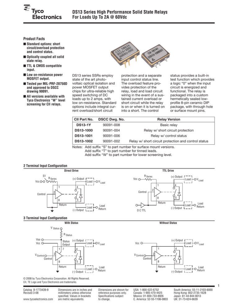
DS13 series SSRs employ
state of the art photovoltaic optical isolation and
power MOSFET output
chips for ultra-reliable high
speed switching of DC
loads up to 2 amps, with
low on-resistance. Standard
options include integral current overload/short circuit
protection and a separate
input control status line.
The overload feature provides protection of the
relay, load and load circuit
wiring in the event of a sustained current overload or
short circuit while the relay
is on or when it is turned on
into a short. The control
CII Part No.
DSCC Dwg. No.
status provides a built-in
test function which provides
a logic “0” when the input
circuit is energized and
functional. The relay is
packaged into a custom
hermetically sealed lowprofile 8-pin ceramic DIP
package, with through hole
or surface mount pins.
Relay Version
DS13-1Y
90091-008
Basic relay
DS13-1000
90091-004
Relay w/ short circuit protection
DS13-1001
90091-006
Relay w/ control status
DS13-1002
90091-002
Relay w/ short circuit protection and control status
Notes: Add suffix “S” to part number for surface mount versions.
Add suffix “T” to part number for tinned leads.
Add suffix “W” to part number for lower screening level.
2 Terminal Input Configuration
Direct Drive
S1
R Series
TTL Drive
(+) Output
Vcc
Load
V Load
Vcc
4
1
Control
2
Control
R Series
1
4
8
5
Return
Return
Load
(-) Output
Load
Return
Load
V Load
Load
Load
Return
Load
V Load
Load
Load
Return
2
5
8
(+) Output
(-) Output
O C TTL
3 Terminal Input Configuration
With Status
Without Status
V Status
R Status
Vso
Vcc
Status (+) Output
Output
1 7
(+) Output
Load
V Load
Vcc
4
1
4
8
5
2
V Control
Control
2
V Control
Control
8
5
Return
Load
(-) Output
Load
Return
Return
(-) Output
© 2008 by Tyco Electronics Corporation. All Rights Reserved.
CII, TE Logo and Tyco Electronics are trademarks.
1
Catalog 8-1773439-9
Revised 3-08
www.tycoelectronics.com
Dimensions are in inches and
millimeters unless otherwise
specified. Values in brackets
are metric equivalents.
Dimensions are shown for
reference purposes only.
Specifications subject
to change.
USA: 1-800-522-6752
Canada: 1-905-470-4425
Mexico: 01-800-733-8926
C. America: 52-55-1106-0803
South America: 55-11-2103-6000
Hong Kong: 852-2735-1628
Japan: 81-44-844-8013
UK: 31-73-624-6639
High Performance Electronic Products
DS13 SSR for loads up to 2A @ 60Vdc (Continued)
Environmental Characteristics
Electrical Specifications (-55°C to +105°C unless otherwise specified)
Ambient Temperature Range:
Operating: -55°C to +105°C.
Storage: -55°C to +125°C.
Input (2 terminal configuration)
Vibration Resistance:
100 G’s, 10-3,000 Hz.
Input supply voltage range (Vcc)
3.8 - 32 Vdc (Notes 1 & 2, Figures 1 & 2)
Input current (max.) @ 5Vdc
15mAdc (Notes 1 & 2, Figures 1 & 2)
Must turn-on voltage
3.8Vdc
Shock Resistance:
1,500 G’s, 0.5 ms pulse.
Must turn-off voltage
1.5Vdc
Reverse voltage protection
-32Vdc
Constant Acceleration Resistance:
5,000 G’s.
Input (3 terminal configuration)
Control voltage range
0 - 18 Vdc
Control current (max.)
240µAdc @ 5V, 1mA @ 18V
Input supply voltage range (Vcc)
3.8 - 32 Vdc (Notes 1 & 2, Figures 1 & 2)
Input current (max.) @ 5Vdc
15mAdc (Notes 1 & 2, Figures 1 & 2)
Mechanical Characteristics
Must turn-on voltage
0.3Vdc
Weight (max.):
.07 oz. (2 grams)
Must turn-off voltage
3.2Vdc
Materials:
Case: DIP, hermetically sealed,
ceramic
Pins: Copper, gold plated
Dielectric Strength (min.)
I/O
1,000V rms
109 ohms
Insulation Resistance (min.) @ 500Vdc
Capacitance (max.)
10pF
Output
Continuous load current (max.) @ 25°C, without short circuit protection
2.0Adc (Figure 5, Note 3)
Continuous load current (max.) @ 25°C, with short circuit protection
1.0Adc (Figure 5, Note 3)
Continuous load voltage (max.)
60Vdc
Transient blocking voltage (max.)
80Vdc (Note 4)
On resistance (max.) @ Tj = 25°C, IL = 100ma, with short circuit protection
0.45 ohm (Note 5, Figure 4)
On resistance (max.) @ Tj = 25°C, IL = 100ma, without short circuit protection
0.22 ohm (Note 5, Figure 4)
Output voltage drop (max.), with short circuit protection
0.6Vdc
Output voltage drop (max.), without short circuit protection
0.75Vdc
Off-state leakage current (max.) @ 60Vdc
100µAdc
Turn-on time (max.)
1.5 ms (Figure 3)
Turn-off time (max.)
.25 ms (Figure 3)
dv/dt (min.)
100V / µs
Electrical system spike
±600Vdc (Note 4)
Junction temperature (max.)
150°C
Thermal resistance (max.), junction to ambient
80°C/W
Thermal resistance (max.), junction to case
20°C/W
Status
Status supply voltage
30Vdc
Status sink current (max.) @ Vstatus≤ 0.3Vdc
2mAdc (Note 7)
Status leakage current (max.) @ 15Vdc
4µAdc
Short Circuit Protection
See Figure 6, Note 7
2
Catalog 8-1773439-9
Revised 3-08
www.tycoelectronics.com
Dimensions are in inches and
millimeters unless otherwise
specified. Values in brackets
are metric equivalents.
Dimensions are shown for
reference purposes only.
Specifications subject
to change.
USA: 1-800-522-6752
Canada: 1-905-470-4425
Mexico: 01-800-733-8926
C. America: 52-55-1106-0803
South America: 55-11-2103-6000
Hong Kong: 852-2735-1628
Japan: 81-44-844-8013
UK: 31-73-624-6639
High Performance Electronic Products
DS13 SSR for loads up to 2A @ 60Vdc (Continued)
Figure 1 - Maximum Input Current vs. Input Voltage
Figure 2 - Series Resistance vs. Vcc Supply Voltage (Note 1)
2000
15
R Series (ohms)
Input Current (mA)
18
12
9
6
1500
1000
500
3
0
0
0
10 15 20 25 30 40 50
5
60
0
5
10
Figure 3 - Output Turn-on and Turn-off Timing
High
Pin 2
Low
V Output
Off
90%
10% On
Pin 4-5
TOff
TOn
25
30
35
Figure 4 - On-Resistance vs. Temperature (Note 6)
Normalized On Resistance Factor
(NF)
Control
20
Vcc (Volts)
Input Voltage, Vcc (Vdc)
V
15
2.0
1.8
1.6
1.4
1.2
1.0
0.8
0.6
0.4
0.2
25
50
75
100
125
Junction Temperature (°C)
Figure 6 - Typical Current Trip Levels
5
2.0
DS13-1Y
DS13-1001
1.5
1.0
DS13-1000
DS13-1002
0.5
0.0
-55 15 25 35 45 55 65 75 85 95 105 115 125
Surge Current (amps)
Load Current (amps)
Figure 5 - Temperature Derating Curve
Ambient Temperature (°C)
4
3
+25°C
-55°C
2
+105°C
1
0
0.01
0.1
1
10
100
1000
Time (seconds)
3
Catalog 8-1773439-9
Revised 3-08
www.tycoelectronics.com
Dimensions are in inches and
millimeters unless otherwise
specified. Values in brackets
are metric equivalents.
Dimensions are shown for
reference purposes only.
Specifications subject
to change.
USA: 1-800-522-6752
Canada: 1-905-470-4425
Mexico: 01-800-733-8926
C. America: 52-55-1106-0803
South America: 55-11-2103-6000
Hong Kong: 852-2735-1628
Japan: 81-44-844-8013
UK: 31-73-624-6639
High Performance Electronic Products
DS13 SSR for loads up to 2A @ 60Vdc (Continued)
Figure 7 - Outline Dimensions
Through-Hole Mount Version
.010 ± .002
(.25 ± .05)
6 PLS
.560 MAX.
(14.22)
8
7
Surface Mount Version
.560 MAX.
(14.22)
5
8
7
.485 +.010, –.005
.395 MAX. (12.32 +.25, –.13)
(10.03)
.435 MAX.
(11.05)
.400 ± .015
(10.16 ± .38)
1
2
4
TOP INDEX MARK FOR PIN 1
SIDE INDEX MARK FOR PIN 1
.016 +.010, –.005
(.41 +.25, –.13)
6 PLS
.025
(.64)
6 PLS
.155 MAX.
(3.94)
.395 MAX.
(10.03)
.010 ± .002
(.25 ± .05)
6 PLS
.155 MAX.
(3.94)
.036 +.010, –.005
(.91 +.25, –.13)
6 PLS
.125
(3.18)
.100
(2.54)
.125
(3.18)
.300
(7.62)
1
4
2
TOP INDEX MARK FOR PIN 1
SIDE INDEX MARK FOR PIN 1
.150 ± .015
(3.81 ± .38)
6 PLS
.100
(2.54)
5
.300
(7.62)
.018 ± .002
(.46 ± .05)
6 PLS
.018 ± .002
(.46 ± .05)
6 PLS
Notes
1.2 terminal input configuration is compatible with CMOS or open collector TTL (with pull-up resistor). For Vcc levels above 6Vdc, a series limiting resistor is
required. See Fig. 2 for resistor value. Use standard resistor value equal to or less than value form the curve.
2.Vcc = 5Vdc for all tests unless otherwise specified.
3.All DS13 Series relays may drive loads connected to either positive or negative referenced power supply lines. Reversing polarity of output may cause permanent
damage. Inductive loads must be diode suppressed.
4.Transient blocking voltage & electrical system spike tests are performed per MIL-STD-704 (28Vdc systems).
5.To determine the maximum on-resistance at any given junction temperature, multiply on-resistance at 25°C by normalized on-resistance factor from curve (Fig. 4).
6.Overload testing per MIL-R-28750 is constrained to the limits imposed by the short circuit protection requirements of this specification and DSCC drawing 90091.
Load circuit series inductance for “load shorted” mode of operation to be limited to 50mH max. Maximum repetition rate into a shorted load should not exceed 10
Hz. To calculate maximum on-resistance at any temperature, use the following equation: R(on) = R(on) @ 25°C x NF (without short circuit protection) and R(on) =
0.2 x NF + .21 (with short circuit protection) where NF = normalized on-resistance factor from Fig. 4.
7.Proper operation of the status feedback requires a status pull-up resistor. Select the status resistor such that it limits status output current to 2mA: R status = V
status – 0.3V / 2mA.
8-1773439-9–PDF–KRG–3-08
4
www.tycoelectronics.com
Dimensions are in inches and
millimeters unless otherwise
specified. Values in brackets
are metric equivalents.
Dimensions are shown for
reference purposes only.
Specifications subject
to change.
USA: 1-800-522-6752
Canada: 1-905-470-4425
Mexico: 01-800-733-8926
C. America: 52-55-1106-0803
South America: 55-11-2103-6000
Hong Kong: 852-2735-1628
Japan: 81-44-844-8013
UK: 31-73-624-6639


