DATASHEET
MK3754
LOW COST 54 MHZ 3.3 VOLT VCXO
Description
The frequency of the on-chip VCXO is adjusted by an
external control voltage input into pin VIN. Because VIN is a
high impedance input, it can be driven directly from an
PWM RC integrator circuit. Frequency output increases
with VIN voltage input. The usable range of VIN is 0 to 3 V.
The MK3754D and MK3754B are drop-in replacements for
the MK3754S device. Compared to these earlier devices
the MK3754D and MK3754B offer a wider operating
frequency range and improved power supply noise
rejection.
Features
The MK3754 is ICS’ lowest cost, low jitter, high
performance 3.3 Volt VCXO and PLL clock synthesizer
designed to replace expensive 54 MHz VCXOs. The
on-chip Voltage Controlled Crystal Oscillator accepts a 0 to
3.3 V input voltage to vary the output clocks by ±100 ppm.
Using ICS’ patented VCXO and analog/digital
Phase-Locked Loop (PLL) techniques, the device uses an
inexpensive external 13.5 MHz pullable crystal input to
produce a 54 MHz output clock.
• MK3754D and MK3754B are drop-in upgrades to the
earlier MK3754S device
•
•
•
•
•
The MK3754D exhibits a moderate VCXO gain of
120 ppm/V typical, when used with a high quality external
pullable quartz crystal. The MK3754B offers a higher
VCXO gain of 150 ppm/V. The higher intrinsic VCXO gain
of the MK3754B may help compensate for the reduced
pullability of a low quality crystal used in some applications.
However, higher VCXO gain may also increase clock output
phase noise.
Packaged in 8-pin SOIC
Available in Pb (lead) free package
Operating voltage of 3.3 V
Uses an inexpensive 13.500 MHz external crystal
On-chip VCXO (patented) with pull range of 200 ppm
(minimum)
• VCXO turning voltage of 0 to 3.3V
• 12 mA output drive capability at TTL levels
• Advanced, low power, sub-micron CMOS process
MK3754D is Recommended for New Designs.
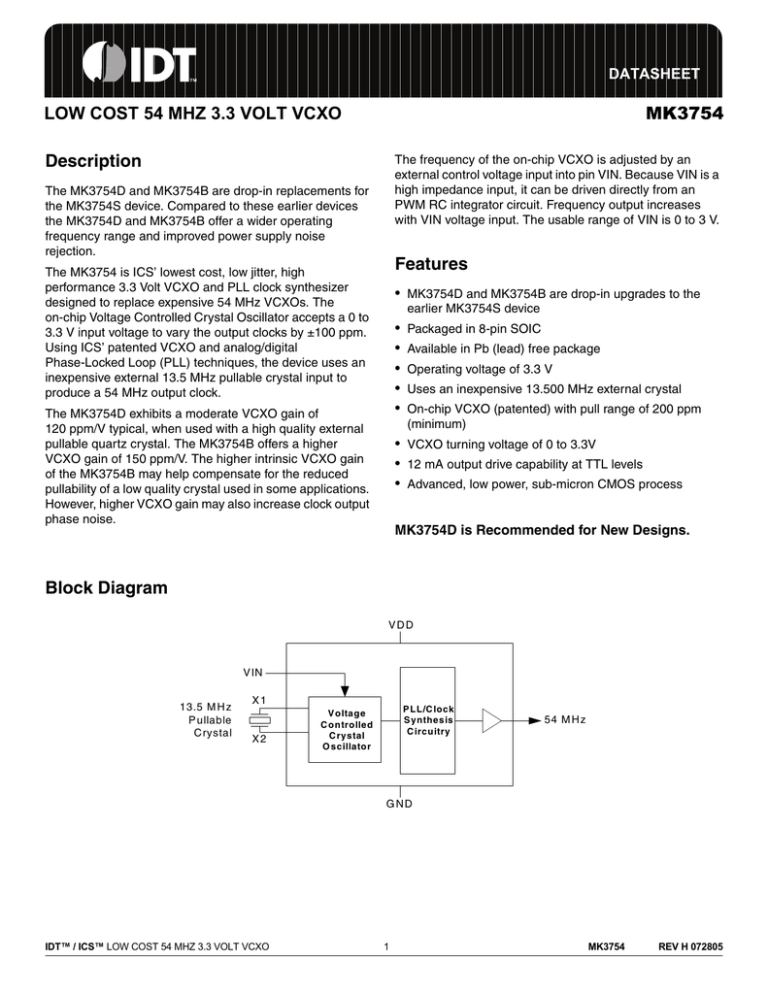
Block Diagram
VDD
V IN
13.5 M H z
P ullable
C rystal
X1
X2
P LL/C lock
S ynthesis
C ircuitry
V oltage
C ontrolled
C rystal
O scillator
54 M H z
GND
IDT™ / ICS™ LOW COST 54 MHZ 3.3 VOLT VCXO
1
MK3754
REV H 072805
MK3754
LOW COST 54 MHZ 3.3 VOLT VCXO
VCXO AND MULTIPLIER
Pin Assignment
X1
1
8
X2
VDD
2
7
GND
VIN
3
6
CLK
GND
4
5
VDD
MK3754S
MK3754B
MK3754D
8 Pin (150 mil) SOIC
Pin Descriptions
Pin
Number
Pin
Name
Pin
Type
1
XI
Input
Crystal connection. Connect to the external pullable crystal.
2
VDD
Power
Connect to +3.3 V (0.01uf decoupling capacitor recommended).
3
VIN
Input
Voltage input to VCXO -- 0 to 3.3 V analog input which controls the
oscillation frequency of the VCXO.
4
GND
Power
Connect to ground.
5
VDD
Power
Connect to +3.3 V (0.01uf decoupling capacitor recommended).
6
CLK
Output 54 MHz clock output.
7
GND
Power
Connect to ground.
8
X2
Input
Crystal connection. Connect to the external pullable crystal.
IDT™ / ICS™ LOW COST 54 MHZ 3.3 VOLT VCXO
Pin Description
2
MK3754
REV H 072805
MK3754
LOW COST 54 MHZ 3.3 VOLT VCXO
VCXO AND MULTIPLIER
External Component Selection
The MK3754 requires a minimum number of external
components for proper operation.
as possible and should be on the same side of the PCB as
the MK3754. There should be no via’s between the crystal
pins and the X1 and X2 device pins. There should be no
signal traces underneath or close to the crystal.
Decoupling Capacitor
Crystal Tuning Load Capacitors
A decoupling capacitor of 0.01 µF must be connected
between VDD (pin 2) and GND (pin 4), as close to these
pins as possible. For optimum device performance, the
decoupling capacitor should be mounted on the component
side of the PCB. Avoid the use of vias in the decoupling
circuit.
The crystal traces should include pads for small fixed
capacitors, one between X1 and ground, and another
between X2 and ground. Stuffing of these capacitors on the
PCB is optional. The need for these capacitors is
determined at system prototype evaluation, and is
influenced by the particular crystal used (manufacture and
frequency) and by PCB layout. The typical required
capacitor value is 1 to 4 pF.
Series Termination Resistor
When the PCB trace between the clock output (CLK, pin 5)
and the load is over 1 inch, series termination should be
used. To series terminate a 50Ω trace (a commonly used
trace impedance) place a 33Ω resistor in series with the
clock line, as close to the clock output pin as possible. The
nominal impedance of the clock output is 20Ω.
The procedure for determining the value of these capacitors
can be found in application note MAN05.
Quartz Crystal
The MK3754 VCXO function consists of the external crystal
and the integrated VCXO oscillator circuit. To assure the
best system performance (frequency pull range) and
reliability, a crystal device with the recommended
parameters (shown below) must be used, and the layout
guidelines discussed in the following section shown must be
followed.
The frequency of oscillation of a quartz crystal is determined
by its “cut” and by the load capacitors connected to it. The
MK3754 incorporates on-chip variable load capacitors that
“pull” (change) the frequency of the crystal. The crystal
specified for use with the MK3754 is designed to have zero
frequency error when the total of on-chip + stray
capacitance is
14 pF.
Recommended Crystal Parameters:
Initial Accuracy at 25°C
Temperature Stability
Aging
Load Capacitance
Shunt Capacitance, C0
C0/C1 Ratio
Equivalent Series Resistance
±20 ppm
±30 ppm
±20 ppm
14 pf
7 pF Max
250 Max
35 Ω Max
The external crystal must be connected as close to the chip
IDT™ / ICS™ LOW COST 54 MHZ 3.3 VOLT VCXO
3
MK3754
REV H 072805
MK3754
LOW COST 54 MHZ 3.3 VOLT VCXO
VCXO AND MULTIPLIER
Absolute Maximum Ratings
Stresses above the ratings listed below can cause permanent damage to the MK3754. These ratings, which are
standard values for ICS commercially rated parts, are stress ratings only. Functional operation of the device at
these or any other conditions above those indicated in the operational sections of the specifications is not implied.
Exposure to absolute maximum rating conditions for extended periods can affect product reliability. Electrical
parameters are guaranteed only over the recommended operating temperature range.
Item
Rating
Supply Voltage, VDD
7V
All Inputs and Outputs
-0.5V to VDD+0.5V
Ambient Operating Temperature
0 to +70°C
Storage Temperature
-65 to +150°C
Soldering Temperature
260°C
Recommended Operation Conditions
Parameter
Ambient Operating Temperature
Power Supply Voltage (measured in respect to GND)
Reference crystal parameters
IDT™ / ICS™ LOW COST 54 MHZ 3.3 VOLT VCXO
Min.
Typ.
Max.
Units
0
–
+70
°C
+3.45
V
+3.15
Refer to page 3
4
MK3754
REV H 072805
MK3754
LOW COST 54 MHZ 3.3 VOLT VCXO
VCXO AND MULTIPLIER
DC Electrical Characteristics
VDD=3.3 V ±5% , Ambient temperature 0 to +70°C, unless stated otherwise
Parameter
Symbol
Conditions
Operating Voltage
VDD
Output High Voltage
VOH
IOH = -12 mA
Output Low Voltage
VOL
IOL = 12 mA
Output High Voltage (CMOS
Level)
VOH
IOH = -4 mA
Operating Supply Current
IDD
No load
Short Circuit Current
IOS
VIN, VCXO Control Voltage
VIA
Min.
Typ.
3.15
Max.
Units
3.45
V
2.4
V
0.4
V
VDD-0.4
V
9
mA
±50
mA
0
3.3
V
AC Electrical Characteristics
VDD = 3.3 V ±5%, Ambient Temperature 0 to +70° C, unless stated otherwise
Parameter
Symbol
Conditions
Min.
Typ.
Max. Units
Crystal Pullability
MK3754D and
MK3754B
FP
0V< VIN < 3.3 V, Note 1
+ 115
ppm
MK3754S
FP
0V< VIN < 3.3 V, Note 1
+ 100
ppm
VCXO Gain
MK3754D
VIN = VDD/2 + 1 V, Note 1
120
ppm/V
MK3754B
VIN = VDD/2 + 1 V, Note 1
150
ppm/V
MK3754S
VIN = VDD/2 + 1 V, Note 1
100
ppm/V
Output Rise Time
tOR
0.8 to 2.0 V, CL=15 pF
1.5
ns
Output Fall Time
tOF
2.0 to 0.8 V, CL=15 pF
1.5
ns
Output Clock Duty Cycle
tD
Measured at 1.4 V, CL=15 pF
55
%
Maximum Output Jitter,
short term
tJ
CL=15 pF
45
50
100
ps
Note 1: External crystal device must conform with Pullable Crystal Specifications listed on page 3.
IDT™ / ICS™ LOW COST 54 MHZ 3.3 VOLT VCXO
5
MK3754
REV H 072805
MK3754
LOW COST 54 MHZ 3.3 VOLT VCXO
VCXO AND MULTIPLIER
Package Outline and Package Dimensions (8-pin SOIC, 150 Mil. Narrow Body)
Package dimensions are kept current with JEDEC Publication No. 95
Index
Area
E H
Pin 1
h x 45 0
D
A
Q
Symbol
Millimeters
Min
Max
Inches*
Min
Max
A
A1
B
C
D
E
e
H
h
L
a
1.35
1.75
1.10
0.25
0.33
0.51
0.19
0.25
4.80
5.00
3.80
4.00
1.27 Basic
5.80
6.20
0.25
0.50
0.40
1.27
0°
8°
0.0532 0.0688
0.0040 0.0098
0.013
0.020
0.0075 0.0098
.1890
.1968
0.1497 0.1574
0.050 Basic
0.2284 0.2440
0.010
0.020
0.016
0.050
0°
8°
*For reference only. Controlling dimensions in mm.
c
e
b
Ordering Information
Part/Order Number (Note 1)
Marking
Shipping Packaging
Package
Temperature
MK3754D
MK3754DTR
MK3754DLF
MK3754DLFTR
MK3754B
MK3754BTR
MK3754BLF
MK3754BLFTR
MK3754S
MK3754STR
MK3754SLF
MK3754SLFTR
MK3754D
MK3754D
3754DLF
3754DLF
MK3754B
MK3754B
3754BLF
3754BLF
MK3754S
MK3754S
3754SLF
3754SLF
Tubes
Tape and Reel
Tubes
Tape and Reel
Tubes
Tape and Reel
Tubes
Tape and Reel
Tubes
Tape and Reel
Tubes
Tape and Reel
8-pin SOIC
8-pin SOIC
8-pin SOIC
8-pin SOIC
8-pin SOIC
8-pin SOIC
8-pin SOIC
8-pin SOIC
8-pin SOIC
8-pin SOIC
8-pin SOIC
8-pin SOIC
0 to +70° C
0 to +70° C
0 to +70° C
0 to +70° C
0 to +70° C
0 to +70° C
0 to +70° C
0 to +70° C
0 to +70° C
0 to +70° C
0 to +70° C
0 to +70° C
Parts that are ordered with a "LF" suffix to the part number are the Pb-Free configuration and are RoHS compliant.
Note 1: MK3754D and MK3754DLF are recommended for new designs. Call factory for information on MK3754S.
While the information presented herein has been checked for both accuracy and reliability, Integrated Circuit Systems (ICS) assumes no
responsibility for either its use or for the infringement of any patents or other rights of third parties, which would result from its use. No
other circuits, patents, or licenses are implied. This product is intended for use in normal commercial applications. Any other applications
such as those requiring extended temperature range, high reliability, or other extraordinary environmental requirements are not
recommended without additional processing by ICS. ICS reserves the right to change any circuitry or specifications without notice. ICS
does not authorize or warrant any ICS product for use in life support devices or critical medical instruments.
IDT™ / ICS™ LOW COST 54 MHZ 3.3 VOLT VCXO
6
MK3754
REV H 072805
MK3754
LOW COST 54 MHZ 3.3 VOLT VCXO
VCXO AND MULTIPLIER
Innovate with IDT and accelerate your future networks. Contact:
www.IDT.com
For Sales
For Tech Support
800-345-7015
408-284-8200
Fax: 408-284-2775
<product line email>
<product line phone>
Corporate Headquarters
Asia Pacific and Japan
Europe
Integrated Device Technology, Inc.
6024 Silver Creek Valley Road
San Jose, CA 95138
United States
800 345 7015
+408 284 8200 (outside U.S.)
Integrated Device Technology
Singapore (1997) Pte. Ltd.
Reg. No. 199707558G
435 Orchard Road
#20-03 Wisma Atria
Singapore 238877
+65 6 887 5505
IDT Europe, Limited
Prime House
Barnett Wood Lane
Leatherhead, Surrey
United Kingdom KT22 7DE
+44 1372 363 339
© 2006 Integrated Device Technology, Inc. All rights reserved. Product specifications subject to change without notice. IDT and the IDT logo are trademarks of Integrated Device
Technology, Inc. Accelerated Thinking is a service mark of Integrated Device Technology, Inc. All other brands, product names and marks are or may be trademarks or registered
trademarks used to identify products or services of their respective owners.
Printed in USA


