DATASHEET
ICS726A
12 TO 36 MHZ 6TSOT VCXO
Description
Features
Used in conjunction with an external pullable quartz crystal,
this monolithic integrated circuit replaces more costly
hybrid (canned) VCXO devices. The ICS726A is designed
primarily for data and clock recovery applications such as
ADSL modems, set-top box receivers, and telecom
systems.
• Uses an inexpensive 12 to 36 MHz external crystal
• Output frequency range of 12 to 36 MHz
• On-chip VCXO with guaranteed pull range of ±115 ppm
minimum
• VCXO tuning voltage 0 to 3.3 V
• Packaged in 6-pin TSOT
• Pb (lead) free package
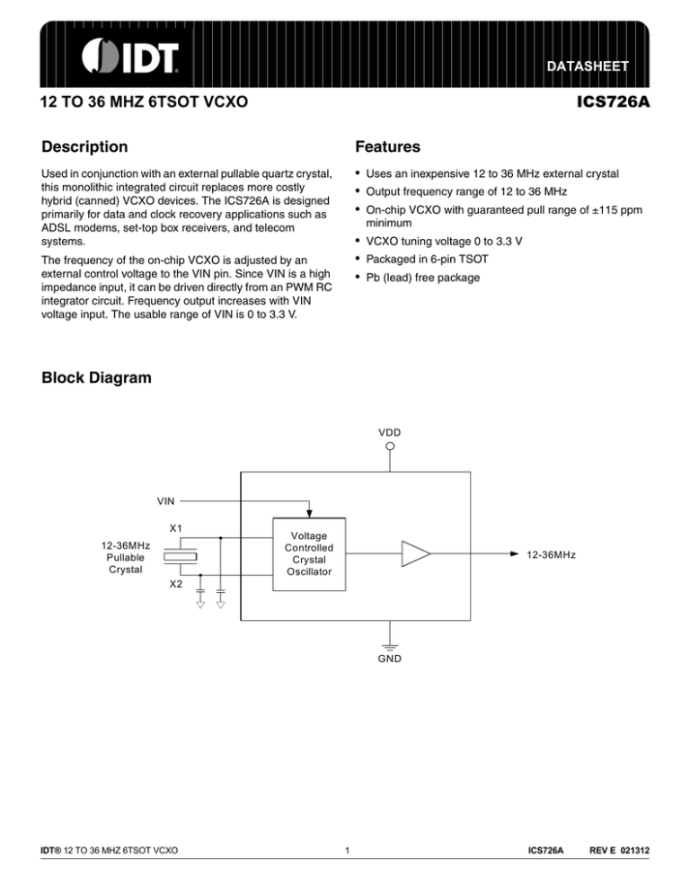
The frequency of the on-chip VCXO is adjusted by an
external control voltage to the VIN pin. Since VIN is a high
impedance input, it can be driven directly from an PWM RC
integrator circuit. Frequency output increases with VIN
voltage input. The usable range of VIN is 0 to 3.3 V.
Block Diagram
VDD
VIN
X1
12-36MHz
Pullable
Crystal
Voltage
Controlled
Crystal
Oscillator
12-36MHz
X2
GND
IDT® 12 TO 36 MHZ 6TSOT VCXO
1
ICS726A
REV E 021312
ICS726A
12 TO 36 MHZ 6TSOT VCXO
VCXO
Pin Assignment
X2
1
6
X1
GND
2
5
VI N
CLK
3
4
VDD
T S OT - 2 3 - 6
Pin Descriptions
Pin
Number
Pin
Name
Pin
Type
Pin Description
1
X2
Input
Crystal connection. Connect to the external pullable crystal.
2
GND
Power
Connect to ground.
3
CLK
Output
VCXO CMOS level clock output at the frequency of the crystal.
4
VDD
Power
Connect to +3.3 V (0.01µf decoupling capacitor recommended).
5
VIN
Input
Voltage input to VCXO — 0 to 3.3 V analog input which controls the
oscillation frequency of the VCXO.
6
XI
Input
Crystal connection. Connect to the external pullable crystal.
External Component Selection
reliability, a crystal device with the recommended
parameters (shown below) must be used, and the layout
guidelines discussed in the following section shown must be
followed.
The ICS726A requires a minimum number of external
components for proper operation.
The frequency of oscillation of a quartz crystal is determined
by its “cut” and by the load capacitors connected to it. The
ICS726A incorporates on-chip variable load capacitors that
“pull” (change) the frequency of the crystal. The crystal
specified for use with the ICS726A is designed to have zero
frequency error when the total of on-chip + stray
capacitance is 8.9 pF.
Decoupling Capacitor
A decoupling capacitor of 0.01µF must be connected
between VDD (pin 4) and GND (pin 2), as close to these
pins as possible. For optimum device performance, the
decoupling capacitor should be mounted on the component
side of the PCB. Avoid the use of vias in the decoupling
circuit.
Required Crystal Parameters:
Series Termination Resistor
Nominal Frequency
as required MHz
Initial Accuracy at 25° C
-20 min/+20 max ppm
Temperature Stability
-30 min/+30 max ppm
Aging, 1st year
-5 min/+5 max ppm
Aging, 10 years
-20 min/+20 max ppm
Operating Temp. Range, °C
0 min/+25 typ/+70 max
or
Operating Temp. Range, °C -40 min/+25 typ/+85 max
Load Capacitance
8.6 pf
Shunt Capacitance, C0
7 pF Max
C0/C1 Ratio
270 Max
Equivalent Series Resistance
35 Ω Max
When the PCB trace between the clock output (CLK, pin 3)
and the load is over 1 inch, series termination should be
used. To series terminate a 50Ω trace (a commonly used
trace impedance) place a 33Ω resistor in series with the
clock line, as close to the clock output pin as possible. The
nominal impedance of the clock output is 20Ω.
Quartz Crystal
The ICS726A VCXO function consists of the external crystal
and the integrated VCXO oscillator circuit. To assure the
best system performance (frequency pull range) and
IDT® 12 TO 36 MHZ 6TSOT VCXO
2
ICS726A
REV E 021312
ICS726A
12 TO 36 MHZ 6TSOT VCXO
VCXO
The third overtone mode of the crystal and all spurs must be
>100 ppm distant from the 3x fundamental resonance
measured with a physical load of 8.6pF.
The value for each of these caps (in pF) is given by:
The external crystal must be connected as close to the chip
as possible and should be on the same side of the PCB as
the ICS726A. There should be no vias between the crystal
pins and the X1 and X2 device pins. There should be no
signal traces underneath or close to the crystal. See
application note MAN05.
Trim sensitivity is a parameter which can be supplied by your
crystal vendor or calculated using the following formula:
= 2 x (centering error)/ (trim sensitivity)
Crystal Tuning Load Capacitors
The crystal traces should include pads for small fixed
capacitors, one between X1 and ground, and another
between X2 and ground. The need for these capacitors is
determined at system prototype evaluation, and is
influenced by the particular crystal used (manufacture and
frequency) and by PCB layout. The typical required
capacitor value is 1 to 4 pF.
To determine the value of the crystal capacitors:
1. Connect VDD of the ICS726A to 3.3 V. Connect pin 5of
the ICS726A to the second power supply. Adjust thevoltage
on pin 5 to 0V. Measure and record the frequency ofthe CLK
output. (f0V)
2. Adjust the voltage on pin 5 to 3.3 V. Measure and record
the frequency of the same output. (fhigh)
Errorxtal = actual initial accuracy (in ppm) of the crystal being
measured.
If the centering error is less than ±25 ppm, no adjustment is
needed. If the centering error is more than 25 ppm negative,
the PC board has excessive stray capacitance and a new
PCB layout should be considered to reduce stray
capacitance. (Alternately, the crystal may be re-specified to
a higher load capacitance. Contact IDT for details.) If the
centering error is more than 25 ppm positive, add identical
fixed centering capacitors from each crystal pin to ground.
IDT® 12 TO 36 MHZ 6TSOT VCXO
3
ICS726A
REV E 021312
ICS726A
12 TO 36 MHZ 6TSOT VCXO
VCXO
Absolute Maximum Ratings
Stresses above the ratings listed below can cause permanent damage to the ICS726A. These ratings, which are
standard values for IDT commercially rated parts, are stress ratings only. Functional operation of the device at these
or any other conditions above those indicated in the operational sections of the specifications is not implied.
Exposure to absolute maximum rating conditions for extended periods can affect product reliability. Electrical
parameters are guaranteed only over the recommended operating temperature range.
Item
Rating
Supply Voltage, VDD
7V
All Inputs and Outputs
-0.5 V to VDD+0.5 V
Ambient Operating Temperature
0 to +70° C
Storage Temperature
-65 to +150° C
Soldering Temperature
260° C
Recommended Operating Conditions
Parameter
Min.
Max.
Units
0
+70
°C
+3.15
+3.45
V
Ambient Operating Temperature
Power Supply Voltage (measured in respect to GND)
Typ.
Reference crystal parameters
Refer to page 3
DC Electrical Characteristics
VDD = 3.3 V ±5% , Ambient temperature 0 to +70° C, unless stated otherwise
Parameter
Symbol
Conditions
Operating Voltage
VDD
Output High Voltage
VOH
IOH = -12 mA
Output Low Voltage
VOL
IOL = 12 mA
Output High Voltage (CMOS
Level)
VOH
IOH = -4 mA
Operating Supply Current
IDD
Output = 12 MHz,
no load
Short Circuit Current
IOS
VIN, VCXO Control Voltage
VIA
IDT® 12 TO 36 MHZ 6TSOT VCXO
Min.
Typ.
3.15
Units
3.45
V
2.4
V
0.4
VDD-0.4
0
4
Max.
V
V
5
mA
±50
mA
3.3
ICS726A
V
REV E 021312
ICS726A
12 TO 36 MHZ 6TSOT VCXO
VCXO
AC Electrical Characteristics
VDD = 3.3 V ±5%, Ambient Temperature 0 to +70° C, unless stated otherwise
Parameter
Symbol
Output Frequency
FO
Crystal Pullability,
Note 2
FP
VCXO Gain
Conditions
Min.
Typ.
12
0V< VIN < 3.3 V, Note 1
Max. Units
36
±115
MHz
ppm
VIN = VDD/2 ± 1 V, Note 1
140
ppm/V
Output Rise Time
tOR
0.8 to 2.0 V, CL=15 pF
0.8
1.5
ns
Output Fall Time
tOF
2.0 to 0.8 V, CL=15 pF
0.8
1.5
ns
Output Clock Duty
Cycle
tD
Measured at 1.4 V, CL=15 pF
50
60
%
Maximum Output
Jitter, short term
tJ
CL=15 pF
40
100
ps
Note 1: External crystal device must conform with Pullable Crystal Specifications listed on page 3.
Marking Diagram
26AL
Notes:
1. ‘26AL’ denotes part number.
2. “L” denotes Pb (lead) free package.
3. Bottom marking: ‘####’ denotes last 4 digits of lot number
IDT® 12 TO 36 MHZ 6TSOT VCXO
5
ICS726A
REV E 021312
ICS726A
12 TO 36 MHZ 6TSOT VCXO
VCXO
Package Outline and Package Dimensions (6-pin TSOT)
Package dimensions are kept current with JEDEC Publication No. 95
Millimeters
Min
Max
Symbol
A
A1
A2
b
c
D
E
E1
e
e1
L
L1
L2
θ
—
1.00
0.01
0.10
0.84
0.90
0.30
0.45
0.12
0.20
2.90 BASIC
2.80 BASIC
1.60 BASIC
0.95 BASIC
1.90 BASIC
0.30
0.50
0.60 REF.
0.25 BASIC
0°
8°
aaa
—
0.10
Ordering Information
Part / Order Number
Marking
Shipping Packaging
Package
Temperature
726ATLFT
26AL
Tape and Reel
6-pin TSOT
0 to +70° C
“A” denotes revision designator (will not corrrelate with datasheet revision)
"LF" suffix to the part number are the Pb-Free configuration and are RoHS compliant.
While the information presented herein has been checked for both accuracy and reliability, Integrated Device Technology (IDT) assumes
no responsibility for either its use or for the infringement of any patents or other rights of third parties, which would result from its use. No
other circuits, patents, or licenses are implied. This product is intended for use in normal commercial applications. Any other applications
such as those requiring extended temperature range, high reliability, or other extraordinary environmental requirements are not
recommended without additional processing by IDT. IDT reserves the right to change any circuitry or specifications without notice. IDT
does not authorize or warrant any IDT product for use in life support devices or critical medical instruments.
IDT® 12 TO 36 MHZ 6TSOT VCXO
6
ICS726A
REV E 021312
ICS726A
12 TO 36 MHZ 6TSOT VCXO
VCXO
Innovate with IDT and accelerate your future networks. Contact:
www.IDT.com
For Sales
For Tech Support
800-345-7015
408-284-8200
Fax: 408-284-2775
www.idt.com/go/clockhelp
Corporate Headquarters
Integrated Device Technology, Inc.
www.idt.com
© 2012 Integrated Device Technology, Inc. All rights reserved. Product specifications subject to change without notice. IDT and the IDT logo are trademarks of Integrated Device
Technology, Inc. Accelerated Thinking is a service mark of Integrated Device Technology, Inc. All other brands, product names and marks are or may be trademarks or registered
trademarks used to identify products or services of their respective owners.
Printed in USA


