Application Note 1578 LM25575 Evaluation Board
advertisement

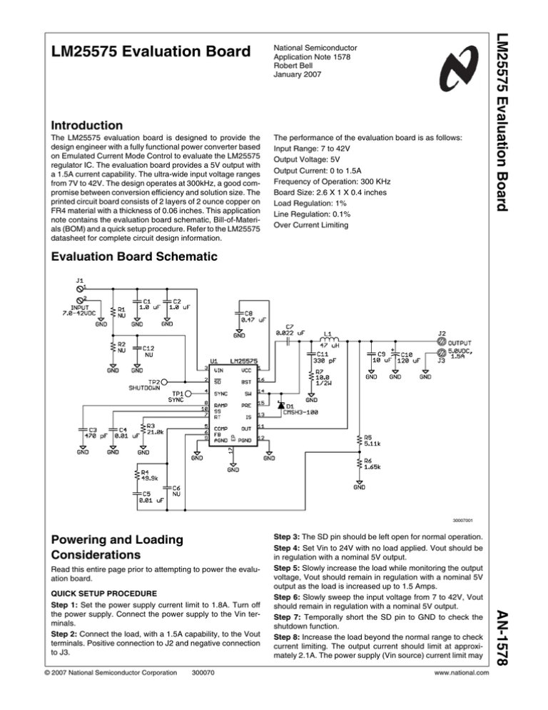
National Semiconductor Application Note 1578 Robert Bell January 2007 Introduction The LM25575 evaluation board is designed to provide the design engineer with a fully functional power converter based on Emulated Current Mode Control to evaluate the LM25575 regulator IC. The evaluation board provides a 5V output with a 1.5A current capability. The ultra-wide input voltage ranges from 7V to 42V. The design operates at 300kHz, a good compromise between conversion efficiency and solution size. The printed circuit board consists of 2 layers of 2 ounce copper on FR4 material with a thickness of 0.06 inches. This application note contains the evaluation board schematic, Bill-of-Materials (BOM) and a quick setup procedure. Refer to the LM25575 datasheet for complete circuit design information. The performance of the evaluation board is as follows: Input Range: 7 to 42V Output Voltage: 5V Output Current: 0 to 1.5A Frequency of Operation: 300 KHz Board Size: 2.6 X 1 X 0.4 inches Load Regulation: 1% Line Regulation: 0.1% Over Current Limiting LM25575 Evaluation Board LM25575 Evaluation Board Evaluation Board Schematic 30007001 Powering and Loading Considerations Read this entire page prior to attempting to power the evaluation board. © 2007 National Semiconductor Corporation 300070 www.national.com AN-1578 QUICK SETUP PROCEDURE Step 1: Set the power supply current limit to 1.8A. Turn off the power supply. Connect the power supply to the Vin terminals. Step 2: Connect the load, with a 1.5A capability, to the Vout terminals. Positive connection to J2 and negative connection to J3. Step 3: The SD pin should be left open for normal operation. Step 4: Set Vin to 24V with no load applied. Vout should be in regulation with a nominal 5V output. Step 5: Slowly increase the load while monitoring the output voltage, Vout should remain in regulation with a nominal 5V output as the load is increased up to 1.5 Amps. Step 6: Slowly sweep the input voltage from 7 to 42V, Vout should remain in regulation with a nominal 5V output. Step 7: Temporally short the SD pin to GND to check the shutdown function. Step 8: Increase the load beyond the normal range to check current limiting. The output current should limit at approximately 2.1A. The power supply (Vin source) current limit may AN-1578 need to be increased for this step. Cooling is critical during this step. TURN-ON WAVEFORM When applying power to the LM25575 evaluation board a certain soft-start sequence occurs. Figure 2 shows the output voltage during a typical start-up sequence. AIR FLOW Prolonged operation with high input voltage at full power will cause the thermal shutdown circuit within the regulator IC to activate. A stand-alone fan with at lease 200 LFM should always be provided. POWERING UP Using the shutdown pin provided will allow powering up the source supply with the current level set low. It is suggested that the load be kept low during the first power up. Set the current limit of the source supply to provide about 1.5 times the anticipated wattage of the load. As you remove the connection from the shutdown pin to ground, immediately check for 5 volts at the output. A quick efficiency check is the best way to confirm that everything is operating properly. If something is amiss you can be reasonably sure that it will affect the efficiency adversely. Few parameters can be incorrect in a switching power supply without creating losses and potentially damaging heat. 30007003 Conditions: Input Voltage = 36VDC, Output Current = 1A Trace 1: Output Voltage Volts/div = 2V Horizontal Resolution = 500 µsec/div OVER CURRENT PROTECTION The evaluation board is configured with over-current protection. The output current is limited to approximately 2.1A. The thermal stress is quite severe while in an overloaded condition, limit the duration of the overload and provide sufficient cooling (airflow). FIGURE 2. OUTPUT RIPPLE WAVEFORM Figure 3 shows the output voltage ripple. This measurement was taken with a very short ground clip and 20MHZ bandwidth limiting. SYNCHRONIZATION A SYNC pin has been provided on the evaluation board. This pin can be used to synchronize the regulator to an external clock or multiple evaluation boards can be synchronized together by connecting their SYNC pins together. Refer to the LM25575 datasheet for complete information. Performance Characteristics EFFICIENCY PLOTS Figure 1 shows the conversion efficiency versus output current for several input voltage conditions. 30007004 Conditions: Input Voltage = 36VDC Output Current = 1A Bandwidth Limit = 20 MHz Trace 1: Output Ripple Voltage Volts/div = 50 mV Horizontal Resolution = 2 µsec/div FIGURE 3. 30007002 FIGURE 1. www.national.com 2 AN-1578 Layout and Bill of Materials The Bill of Materials is shown below, including the manufacturer and part number. TABLE 1. 5V, 1.5A Demo Board Bill of Materials ITEM PART NUMBER DESCRIPTION VALUE C 1 C3225X7R2A105M CAPACITOR, CER, TDK C 2 C3225X7R2A105M CAPACITOR, CER, TDK C 3 C0805A471K1GAC CAPACITOR, CER, KEMET 470p, 100V C 4 C2012X7R2A103K CAPACITOR, CER, TDK 0.01µ, 100V C 5 C2012X7R2A103K CAPACITOR, CER, TDK 0.01µ, 100V C 6 OPEN NOT USED C 7 C2012X7R2A223K CAPACITOR, CER, TDK 0.022µ, 100V C 8 C2012X7R1C474M CAPACITOR, CER, TDK 0.47µ, 16V C 9 C3225X7R1C106M CAPACITOR, CER, TDK C 10 APXE6R3ARA121ME61G CAPACITOR, AL, NIPPON 120µ, 6.3V C 11 C0805C331G1GAC CAPACITOR, CER, KEMET 330p, 100V C 12 OPEN NOT USED D 1 CMSH3-60 DIODE, 60V, CENTRAL L 1 DR125-470 INDUCTOR, COOPER R 1 OPEN NOT USED R 2 OPEN NOT USED R 3 CRCW08052102F RESISTOR 21kΩ R 4 CRCW08054992F RESISTOR 49.9kΩ R 5 CRCW08055111F RESISTOR 5.11kΩ R 6 CRCW08051651F RESISTOR 1.65kΩ R 7 CRCW2512100J RESISTOR 10, 1W U 1 LM25575 REGULATOR, NATIONAL SEMICONDUCTOR 3 1µ, 100V 1µ, 100V 10µ, 16V 47µH www.national.com AN-1578 PCB Layout 30007005 Component Side 30007006 Solder Side 30007007 Silkscreen www.national.com 4 AN-1578 Notes 5 www.national.com LM25575 Evaluation Board Notes THE CONTENTS OF THIS DOCUMENT ARE PROVIDED IN CONNECTION WITH NATIONAL SEMICONDUCTOR CORPORATION (“NATIONAL”) PRODUCTS. NATIONAL MAKES NO REPRESENTATIONS OR WARRANTIES WITH RESPECT TO THE ACCURACY OR COMPLETENESS OF THE CONTENTS OF THIS PUBLICATION AND RESERVES THE RIGHT TO MAKE CHANGES TO SPECIFICATIONS AND PRODUCT DESCRIPTIONS AT ANY TIME WITHOUT NOTICE. NO LICENSE, WHETHER EXPRESS, IMPLIED, ARISING BY ESTOPPEL OR OTHERWISE, TO ANY INTELLECTUAL PROPERTY RIGHTS IS GRANTED BY THIS DOCUMENT. TESTING AND OTHER QUALITY CONTROLS ARE USED TO THE EXTENT NATIONAL DEEMS NECESSARY TO SUPPORT NATIONAL’S PRODUCT WARRANTY. EXCEPT WHERE MANDATED BY GOVERNMENT REQUIREMENTS, TESTING OF ALL PARAMETERS OF EACH PRODUCT IS NOT NECESSARILY PERFORMED. NATIONAL ASSUMES NO LIABILITY FOR APPLICATIONS ASSISTANCE OR BUYER PRODUCT DESIGN. BUYERS ARE RESPONSIBLE FOR THEIR PRODUCTS AND APPLICATIONS USING NATIONAL COMPONENTS. PRIOR TO USING OR DISTRIBUTING ANY PRODUCTS THAT INCLUDE NATIONAL COMPONENTS, BUYERS SHOULD PROVIDE ADEQUATE DESIGN, TESTING AND OPERATING SAFEGUARDS. EXCEPT AS PROVIDED IN NATIONAL’S TERMS AND CONDITIONS OF SALE FOR SUCH PRODUCTS, NATIONAL ASSUMES NO LIABILITY WHATSOEVER, AND NATIONAL DISCLAIMS ANY EXPRESS OR IMPLIED WARRANTY RELATING TO THE SALE AND/OR USE OF NATIONAL PRODUCTS INCLUDING LIABILITY OR WARRANTIES RELATING TO FITNESS FOR A PARTICULAR PURPOSE, MERCHANTABILITY, OR INFRINGEMENT OF ANY PATENT, COPYRIGHT OR OTHER INTELLECTUAL PROPERTY RIGHT. LIFE SUPPORT POLICY NATIONAL’S PRODUCTS ARE NOT AUTHORIZED FOR USE AS CRITICAL COMPONENTS IN LIFE SUPPORT DEVICES OR SYSTEMS WITHOUT THE EXPRESS PRIOR WRITTEN APPROVAL OF THE CHIEF EXECUTIVE OFFICER AND GENERAL COUNSEL OF NATIONAL SEMICONDUCTOR CORPORATION. As used herein: Life support devices or systems are devices which (a) are intended for surgical implant into the body, or (b) support or sustain life and whose failure to perform when properly used in accordance with instructions for use provided in the labeling can be reasonably expected to result in a significant injury to the user. A critical component is any component in a life support device or system whose failure to perform can be reasonably expected to cause the failure of the life support device or system or to affect its safety or effectiveness. National Semiconductor and the National Semiconductor logo are registered trademarks of National Semiconductor Corporation. All other brand or product names may be trademarks or registered trademarks of their respective holders. Copyright© 2007 National Semiconductor Corporation AN-1578 For the most current product information visit us at www.national.com National Semiconductor Americas Customer Support Center Email: new.feedback@nsc.com Tel: 1-800-272-9959 www.national.com National Semiconductor Europe Customer Support Center Fax: +49 (0) 180-530-85-86 Email: europe.support@nsc.com Deutsch Tel: +49 (0) 69 9508 6208 English Tel: +49 (0) 870 24 0 2171 Français Tel: +33 (0) 1 41 91 8790 National Semiconductor Asia Pacific Customer Support Center Email: ap.support@nsc.com National Semiconductor Japan Customer Support Center Fax: 81-3-5639-7507 Email: jpn.feedback@nsc.com Tel: 81-3-5639-7560


