Exercises 3 Logic Design
advertisement

Exercises 3
Logic Design
Computer Organization and Components / Datorteknik och komponenter (IS1500), 9 hp
(not part of IS1200, but can be used for review)
KTH Royal Institute of Technology
Thursday 14th January, 2016
Gates and Boolean Algebra
1. Draw the symbols and write out the truth tables for the following logic gates:
AND, OR, NOT, NAND, NOR, XOR
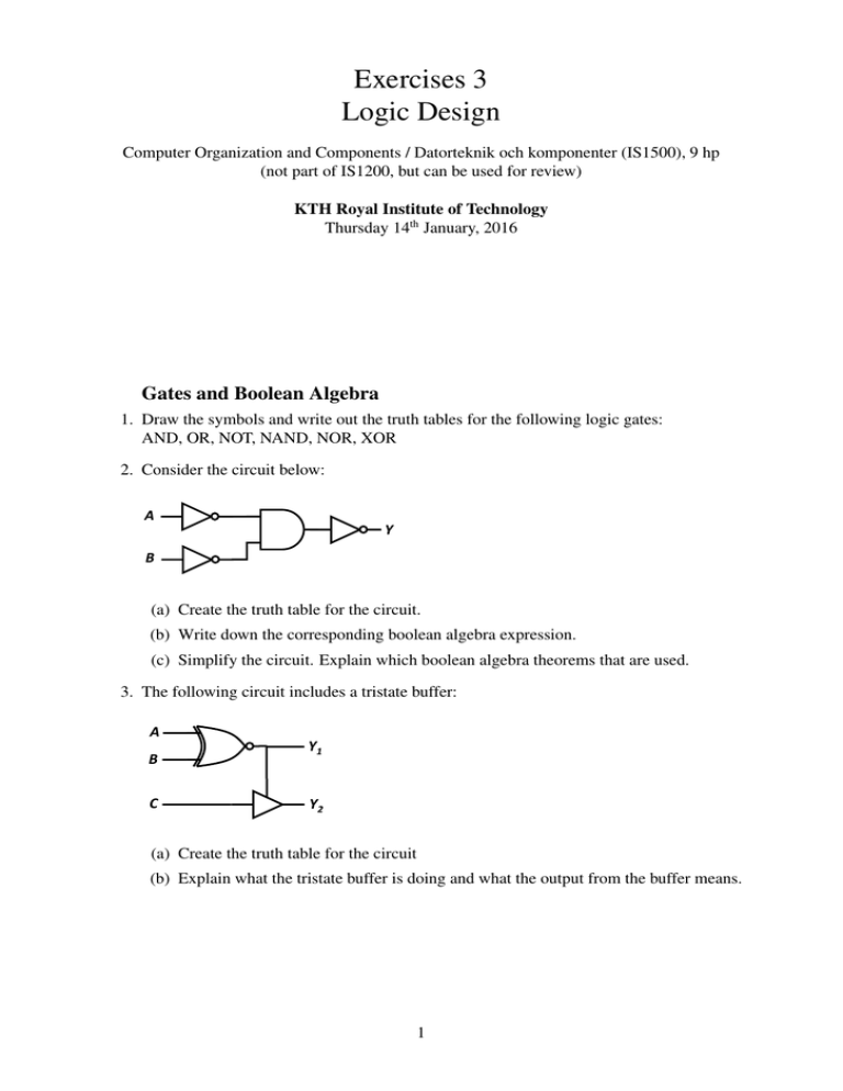
2. Consider the circuit below:
A!"
Y"
B!"
(a) Create the truth table for the circuit.
(b) Write down the corresponding boolean algebra expression.
(c) Simplify the circuit. Explain which boolean algebra theorems that are used.
3. The following circuit includes a tristate buffer:
A
Y1"
B
C
Y2"
(a) Create the truth table for the circuit
B what the tristate buffer is doing and what the output from the buffer means.
(b) Explain
A!"
Y"
B!"
1
4. Consider the following truth table.
S!
0"
0"
0"
0"
1"
1"
1"
1"
Y"
A"
0"
0"
1"
1"
0"
0"
1"
1"
B"
0"
1"
0"
1"
0"
1"
0"
1"
Y!
0"
1"
0"
1"
0"
0"
1"
1"
(a) Create the corresponding boolean expression in sum-of-products form.
(b) Simplify the expression using the boolean theorems presented at Lecture 7.
Clearly state which theorems that you are using.
(c) Draw the final circuit in a simple form, that is, reuse as many gates as possible.
Multiplexers, Decoders, and Adders
5. The following tasks concerns a 2:1 multiplexer.
(a) Draw the symbol for the multiplexer.
(b) Create the truth table in a short form, where the “don’t care” symbol “?” is used as
often as possible.
(c) Draw a circuit that gives the same meaning as the above 2:1 multiplexer. The circuit
should consist of exactly 2 AND-gates, 1 OR-gate, and 1 NOT-gate.
(d) How does this circuit compare to the solution of exercise 4c.
6. Decoders.
(a) Draw a figure for a 3:8 decoder.
(b) Write out the truth table for a 2:4 decoder.
(c) Explain the meaning of the numbers that determine the size of the two encoders 3:8
and 2:4.
(d) Create a circuit consisting of AND-gates, OR-gates, and NOT-gates that defines a
2:4 decoder.
7. Assume that you want to create a 4:1 multiplex where the data input/output ports have
8-bit bus width. Draw the multiplexer. Note that you must clearly show the bus width of
the wires.
8. Construct a circuit that takes a 6-bit input A and outputs a 6-bit signal Y , where the output
is A multiplied by value 3. You should use 1-bit full adders and basic gates.
2
Y1"
Y2"
S! A" B" Y!
0" 0" 0" 0"
0" 0" 1" 1"
0" 1" 0" 0"
0" 1" 1" 1"
1" 0" 0" 0"
1" 0"
1" 0"
9. Construct a 4-bit
equality comparator
that checks that two input signals A and B are
0"
1"
1"
1"
equal, that is, that each corresponding bit has the same value.
1" 1" 1" 1"
Latches, Flip-Flops, Registers, and Register Files
Y"
10. The following figure shows a SR latch.
R
S
A
Q
Q
S! A" B" Y!
Q
0" Explain
0"
B
0" 0" input.
Construct the truth table for the SR latch, by considering each possible
0" 0" 1" 1"
how and why the signals stabalize for each possible input.
C
Y2"
0" 1" 0" 0"
11. D Flip-Flops
0" 1" 1" 1"
1" 0" 0" 0"
Q
(a) Draw the symbol for a D Flip-Flop with enable signal.
S
1" 0" 1" 0"
(b) Explain what the D Flip-Flop above means and in what way it is different from SR
A!"
1" 1" 0" 1"
latches and D latches.
Y"
1" 1" 1" 1"
Y1"
R
(c) Consider the clock signals below. Assume that the D Flip-flop is activated on the
B!"
rising edge. Draw the output signal Q. Assume that Q is 0 at the beginning of the
example sequence.
CLK!"
EN!"
D!"
3
12. Consider the following circuit where the register is triggered on the rising clock edge.
A$
B$
8"
8"
+$
Cin$
C$
8"
CLK$
CLK$
R1" Y
1$
R2" Y
2$
(a) Assume that register R1 holds value 0x3, register R2 value 0x5, A = 3, B = 0,
and C = 0. Show the signal values for signals Y1 and Y2 for the first 3 clock cycles.
(b) Assume that register R1 holds value 0x10, register R2 value 0x8, A = 2, B = 255,
and C = 1. Show the signal values for signals Y1 and Y2 for the first 3 clock cycles.
13. Consider the following register file. Assume that N = 4 and M = 16.
CLK$
N
CLK$
N
N
R2" Y
2$
M
A1$
A2$
WE3$
RD1$
RD2$
M
M
A3$
WD3$
(a) What is the difference between a register file and a register?
(b) How many ports has the above the register file got? How many input ports and how
many output ports?
(c) What is the total number of bits of data that this register file can store?
(d) Assume the following mapping from addresses to memory values {0x3 7→ 0x3f,
0xa 7→ 0x22, 0x9 7→ 0xe7} is a known state of the register file. Assume further
that A1 = 0xa, A2 = 0x9, A3 = 0x3, WD 3 = 0x53, and WE 3 = 0x1. What
are then the values for RD 1 and RD 2 and what is the new known state of the register
file?
4

