Package - Silicon Power Corporation
advertisement
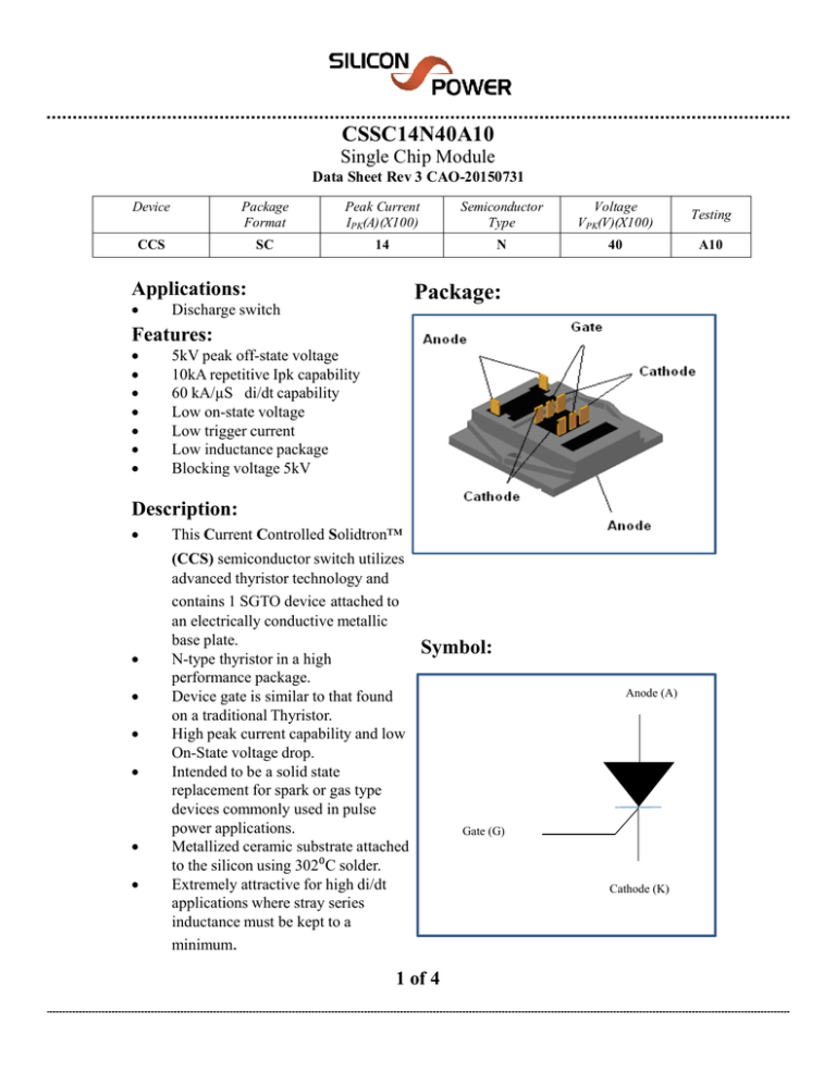
CSSC14N40A10 Single Chip Module Data Sheet Rev 3 CAO-20150731 Device Package Format Peak Current IPK(A)(X100) Semiconductor Type Voltage VPK(V)(X100) Testing CCS SC 14 N 40 A10 Applications: Package: Discharge switch Features: 5kV peak off-state voltage 10kA repetitive Ipk capability 60 kA/µS di/dt capability Low on-state voltage Low trigger current Low inductance package Blocking voltage 5kV Description: This Current Controlled Solidtron™ (CCS) semiconductor switch utilizes advanced thyristor technology and contains 1 SGTO device attached to an electrically conductive metallic base plate. N-type thyristor in a high performance package. Device gate is similar to that found on a traditional Thyristor. High peak current capability and low On-State voltage drop. Intended to be a solid state replacement for spark or gas type devices commonly used in pulse power applications. Metallized ceramic substrate attached to the silicon using 302⁰C solder. Extremely attractive for high di/dt applications where stray series inductance must be kept to a minimum. Symbol: 1 of 4 Anode (A) Gate (G) Cathode (K) Dimensions: Absolute Maximum Ratings Peak off-state voltage Symbol VDRM Value 5 Units kV Peak reverse voltage VRRM -5 V Off-state rate of change of voltage immunity dv/dt 1 kV/µS Continuous anode current at Tj = 125⁰C IA110 100 A Repetitive peak anode current (Pulse Width = 10µ) IASM 10.0 kA Nonrepetitive Peak Anode Current (Pulse Width = 10µ) IASM 14 kA Rate of change of current di/dt 60 kA/µS Peak gate current (1µ) Max. reverse gate-cathode voltage IGpk VGR 100 -9 A V Maximum junction temperature TjM 125 ⁰C 2 of 4 Performance Characteristics ( Tj = 25⁰C unless otherwise specified.) Measurements Performance Ratings Parameters Symbol Min. Typ. Max. Units Anode to cathode breakdown voltage Anode-cathode off-state current VDR 4 5 5.5 kV VGK=0V, IA = 1mA <50 100 µA 100 800 µA VGK=0V, VAK=4000V ID Turn-on threshold current VGK(TH) Gate-cathode leakage current IGK(IKQ) Anode-cathode on-state voltage Turn-on delay time Peak rate of change of current Peak anode current 5 Ton di/dt IP 30 Tj=25⁰C Tj=125⁰C mA VAK=VGK , 1mA, See Note 1 µA VGK=0V, See Note 1 1.7 V 1.9 V IT=400A Ig=500mA 200 60 ns kA/us 20 VT Test Conditions 10 70 kA Tj=25⁰C Tj=125⁰C 0.75 µF Capacitor discharge VAK = 3.95 kV Tj=25⁰C RGK = 10ohms, Ls = 90nH Gate di/dt = 100 A/us Notes: 1. . Measurements made with a 10 Ohm shorting resistor connected between the gate and cathode. 2. Case Exterior Assumed to be 0.002” of 63sn/37pb solder applied directly to cathode bond area of ThinPak. 3. All product specifications and data are subject to change without notice. Devices shall be tested and qualified in their respective applications and circuitry. Depending on the application and circuitry, adjustments to the specifications may be necessary. We strongly recommend consultation of Silicon Power personal prior to using our products in medical, life-saving, or life-sustaining applications and systems. 3 of 4 Packaging and Handling 1. Use thermal grease to mount device to cold plate. 2. Consult factory for mounting torque. 3. Do not exceed 175°C device body temperature when soldering leads of the package or internal package gradation may result. 4. ‘ATTENTION OBSERVE PRECAUTIONS FOR HANDLING ELECTROSTATIC DISCHARGE SENSITIVE DEVICES IN ALL ASSEMBLY AND TEST AREAS’ 5. Shorting resistor RGK is application specific. It can control the gate drive requirements and some device properties. However, RGK = 10 Ohms satisfies most application requirements. 6. All metal surfaces are flash gold over nickel plating for solderability. Test Profile 1. Off State leakage Current at 25° C and 5500V against < 2 uA specification 2. Off State leakage Current at 125° C and 5500V against < 1200 uA specification 3. Gate Integrity at 25° C and 12V applied is measured as Pass or Fail Revision History Revision Number Revision Date Reason For Change 1 2 3 5/20/08 3/05/12 7/31/15 Improved datasheet structure; added performance curves Updated drawing Regeneration to Standard; revision log update 4 of 4
