Preliminary
SIDC30D120E6
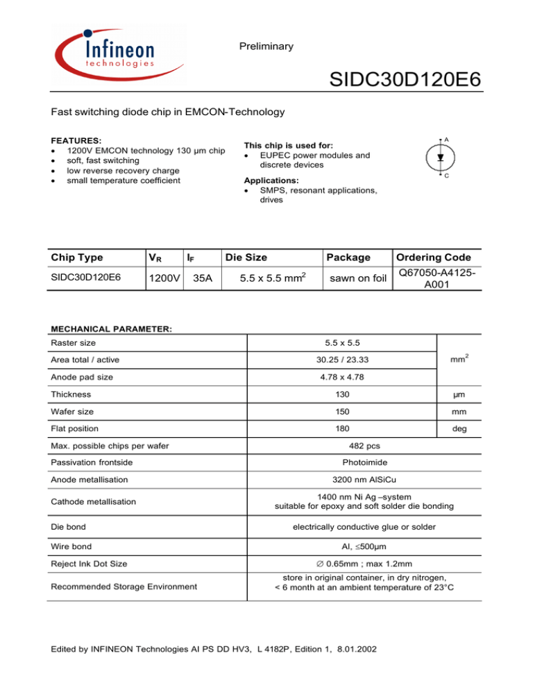
Fast switching diode chip in EMCON-Technology
FEATURES:
• 1200V EMCON technology 130 µm chip
• soft, fast switching
• low reverse recovery charge
• small temperature coefficient
Chip Type
VR
SIDC30D120E6
1200V
IF
35A
A
This chip is used for:
• EUPEC power modules and
discrete devices
C
Applications:
• SMPS, resonant applications,
drives
Die Size
Package
5.5 x 5.5 mm2
sawn on foil
Ordering Code
Q67050-A4125A001
MECHANICAL PARAMETER:
Raster size
Area total / active
Anode pad size
5.5 x 5.5
30.25 / 23.33
mm
2
4.78 x 4.78
Thickness
130
µm
Wafer size
150
mm
Flat position
180
deg
Max. possible chips per wafer
482 pcs
Passivation frontside
Photoimide
Anode metallisation
3200 nm AlSiCu
Cathode metallisation
Die bond
Wire bond
Reject Ink Dot Size
Recommended Storage Environment
1400 nm Ni Ag –system
suitable for epoxy and soft solder die bonding
electrically conductive glue or solder
Al, ≤500µm
∅ 0.65mm ; max 1.2mm
store in original container, in dry nitrogen,
< 6 month at an ambient temperature of 23°C
Edited by INFINEON Technologies AI PS DD HV3, L 4182P, Edition 1, 8.01.2002
Preliminary
SIDC30D120E6
Maximum Ratings
Parameter
Symbol
Repetitive peak reverse voltage
VRRM
Continuous forward current limited by
Tjmax
Single pulse forward current
(depending on wire bond configuration)
Maximum repetitive forward current
limited by Tjmax
Operating junction and storage
temperature
Condition
Value
1200
IF
Unit
V
35
I FSM
tP = 10 ms sinusoidal
A
tbd
I FRM
70
Tj , Ts t g
-55...+150
°C
Static Electrical Characteristics (tested on chip), Tj=25 °C, unless otherwise specified
Parameter
Symbol
Conditions
Reverse leakage current
IR
V R= 1 2 0 0 V
Tj= 2 5 ° C
Cathode-Anode
breakdown Voltage
V Br
I R= 2 m A
Tj= 2 5 ° C
Forward voltage drop
VF
I F= 3 5 A
Tj= 2 5 ° C
Value
min.
Typ.
max.
27
1200
Unit
µA
V
1.9
V
Dynamic Electrical Characteristics, at Tj = 25 °C, unless otherwise specified, tested at component
Parameter
Reverse recovery time
Symbol
t rr1
t rr2
Conditions
I F =35A
di/dt=910A/µs
V R =600V
Value
min.
Tj = 2 5 ° C
Typ.
ns
Tj = 1 2 5 ° C
I F =35A
Tj = 2 5 ° C
36.8
IRRM2
di/dt=910A/µs
VR = 6 0 0 V
Tj = 1 2 5 ° C
46.3
Qrr1
I F =35A
Tj= 2 5 ° C
3.55
Qrr2
di/dt=910A/µs
VR = 6 0 0 V
Tj= 1 2 5 ° C
7.63
Peak rate of fall of reverse di r r 1 /dt
recovery current
di r r 2 /dt
I F =35A
T j = 25 ° C
tbd
di/dt=910A/µs
VR = 6 0 0 V
Tj= 1 2 5 ° C
Softness
S1
I F =35A
Tj= 2 5 ° C
S2
di/dt=910A/µs
VR = 6 0 0 V
Tj= 1 2 5 ° C
Reverse recovery charge
Edited by INFINEON Technologies AI PS DD HV3, L 4182P, Edition 1, 8.01.2002
Unit
tbd
IRRM1
Peak recovery current
max.
A
µC
A / µs
tbd
1
Preliminary
SIDC30D120E6
CHIP DRAWING:
Edited by INFINEON Technologies AI PS DD HV3, L 4182P, Edition 1, 8.01.2002
Preliminary
SIDC30D120E6
FURTHER ELECTRICAL CHARACTERISTICS:
This chip data sheet refers to the
device data sheet
INFINEON TECHNOLOGIES /
EUPEC
tbd
Description:
AQL 0,65 for visual inspection according to failure catalog
Electrostatic Discharge Sensitive Device according to MIL-STD 883
Test-Normen Villach/Prüffeld
Published by
Infineon Technologies AG
Bereich Kommunikation
St.-Martin-Strasse 53
D-81541 München
© Infineon Technologies AG 2000
All Rights Reserved.
Attention please!
The information herein is given to describe certain components and shall not be considered as warranted
characteristics.
Terms of delivery and rights to technical change reserved.
We hereby disclaim any and all warranties, including but not limited to warranties of non-infringement,
regarding circuits, descriptions and charts stated herein.
Infineon Technologies is an approved CECC manufacturer.
Information
For further information on technology, delivery terms and conditions and prices please contact your nearest
Infineon Technologies Office in Germany or our Infineon Technologies Representatives world-wide (see
address list).
Warnings
Due to technical requirements components may contain dangerous substances. For information on the types
in question please contact your nearest Infineon Technologies Office.
Infineon Technologies components may only be used in life-support devices or systems with the express
written approval of Infineon Technologies, if a failure of such components can reasonably be expected to
cause the failure of that life-support device or system, or to affect the safety or effectiveness of that device or
system. Life support devices or systems are intended to be implanted in the human body, or to support
and / or maintain and sustain and / or protect human life. If they fail, it is reasonable to assume that the
health of the user or other persons may be endangered.
Edited by INFINEON Technologies AI PS DD HV3, L 4182P, Edition 1, 8.01.2002
