High-Speed Switching Power Supply Using SiC RESURF JFETs
advertisement
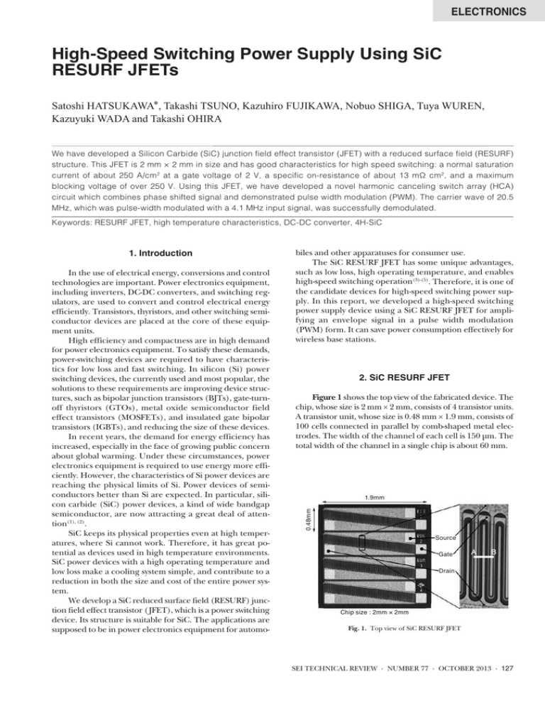
ELECTRONICS High-Speed Switching Power Supply Using SiC RESURF JFETs Satoshi HATSUKAWA*, Takashi TSUNO, Kazuhiro FUJIKAWA, Nobuo SHIGA, Tuya WUREN, Kazuyuki WADA and Takashi OHIRA We have developed a Silicon Carbide (SiC) junction field effect transistor (JFET) with a reduced surface field (RESURF) structure. This JFET is 2 mm × 2 mm in size and has good characteristics for high speed switching: a normal saturation current of about 250 A/cm 2 at a gate voltage of 2 V, a specific on-resistance of about 13 mΩ cm2, and a maximum blocking voltage of over 250 V. Using this JFET, we have developed a novel harmonic canceling switch array (HCA) circuit which combines phase shifted signal and demonstrated pulse width modulation (PWM). The carrier wave of 20.5 MHz, which was pulse-width modulated with a 4.1 MHz input signal, was successfully demodulated. Keywords: RESURF JFET, high temperature characteristics, DC-DC converter, 4H-SiC In the use of electrical energy, conversions and control technologies are important. Power electronics equipment, including inverters, DC-DC converters, and switching regulators, are used to convert and control electrical energy efficiently. Transistors, thyristors, and other switching semiconductor devices are placed at the core of these equipment units. High efficiency and compactness are in high demand for power electronics equipment. To satisfy these demands, power-switching devices are required to have characteristics for low loss and fast switching. In silicon (Si) power switching devices, the currently used and most popular, the solutions to these requirements are improving device structures, such as bipolar junction transistors (BJTs), gate-turnoff thyristors (GTOs), metal oxide semiconductor field effect transistors (MOSFETs), and insulated gate bipolar transistors (IGBTs), and reducing the size of these devices. In recent years, the demand for energy efficiency has increased, especially in the face of growing public concern about global warming. Under these circumstances, power electronics equipment is required to use energy more efficiently. However, the characteristics of Si power devices are reaching the physical limits of Si. Power devices of semiconductors better than Si are expected. In particular, silicon carbide (SiC) power devices, a kind of wide bandgap semiconductor, are now attracting a great deal of attention(1), (2). SiC keeps its physical properties even at high temperatures, where Si cannot work. Therefore, it has great potential as devices used in high temperature environments. SiC power devices with a high operating temperature and low loss make a cooling system simple, and contribute to a reduction in both the size and cost of the entire power system. We develop a SiC reduced surface field (RESURF) junction field effect transistor ( JFET), which is a power switching device. Its structure is suitable for SiC. The applications are supposed to be in power electronics equipment for automo- biles and other apparatuses for consumer use. The SiC RESURF JFET has some unique advantages, such as low loss, high operating temperature, and enables high-speed switching operation(3)-(5). Therefore, it is one of the candidate devices for high-speed switching power supply. In this report, we developed a high-speed switching power supply device using a SiC RESURF JFET for amplifying an envelope signal in a pulse width modulation (PWM) form. It can save power consumption effectively for wireless base stations. 2. SiC RESURF JFET Figure 1 shows the top view of the fabricated device. The chip, whose size is 2 mm × 2 mm, consists of 4 transistor units. A transistor unit, whose size is 0.48 mm × 1.9 mm, consists of 100 cells connected in parallel by comb-shaped metal electrodes. The width of the channel of each cell is 150 µm. The total width of the channel in a single chip is about 60 mm. 1.9mm 0.48mm 1. Introduction Source Gate Drain Chip size : 2mm × 2mm Fig. 1. Top view of SiC RESURF JFET SEI TECHNICAL REVIEW · NUMBER 77 · OCTOBER 2013 · 127 Figure 2 shows a schematic cross-sectional view of the fabricated device along a line between points A and B in Fig. 1. The drift region, between the drain and the gate areas, has a double RESURF structure, which is composed of epitaxial layers based on the super-junction theory. The epitaxial layers consist of active layers (layers 3 and 4), a depletion layer (layer 2) and a field stop layer (layer 1). The thickness and the dopant concentration of each layer are shown in Fig. 2. The drift length, which is the distance between the drain and the gate areas, is 6 µm for a blocking capability of 600 V. The channel (gate) length is 2 µm. The width of the drain and the source fingers is 6 µm. The pitch of the cells is 16 µm. JFETs were fabricated on an 8˚ off (0001)-face n+-type 4H-SiC substrate. The details of the fabrication process were described in our former work(5). Figure 3 shows the typical on-state characteristics of the fabricated transistor. The device shows the current saturation characteristic of FET. It is confirmed that the gate voltage controls the drain current successfully. The on-resistance is calculated to be 250 mΩ from the drain current (Id) when the gate voltage (Vgs) is 2 V and the drain voltage (Vds) is 1 V. Figure 4 shows the blocking characteristics of the fabricated transistor. The gate voltage (Vgs) is -8 V, at which the transistor turns off. The transistor has a measured blocking voltage of more than 250 V. Id [nA] 5 VGS : -8V 4 3 2 1 0 0 50 100 150 200 250 Vds [V] A 2μm 2μm 6μm 6μm 6μm Source Gate Source Drain Gate Source B Fig. 4. Blocking characteristics Layer 4 (p-type) [0.25μm, 2×1017cm -3 ] Layer 3 (n-type) [0.45μm, 2×1017cm -3 ] Load Layer 2 (p-type) [10μm, 7.5×1015cm -3 ] Vds Layer 1 (p-type) [0.5μm, 5×1016cm -3 ] Rg p+-Ion Implantation [dose: 3.9×1014cm -3 ] n+-Ion Implantation [dose: 1.1×1014cm -3 ] Fig. 5. Evaluation circuit for measuring inductive load switching characteristics Fig. 2. Cross-sectional view of RESURF JFET Id [A] Vgs : 6V 4V 15 2V 10 40 20 0 -20 0V -2V 0 -4V -6V 2 4 6 8 10 Vds [V] Fig. 3. Drain current (Id) versus drain voltage (Vds) different values of gate voltage (Vgs) 128 · High-Speed Switching Power Supply Using SiC RESURF JFETs Voltage [V] 60 5 Vds 60 Voltage [V] 20 0 Vgs Gate Driver 4H-SiC Substrate (n+) 100ns Vgs OffàOn (Tf) Vds 40 20 0 -20 60 40 OnàOff (Tr) Vds 20 0 Vgs 5ns -20 Vgs Fig. 6. Switching characteristics 5ns Figure 5 shows the testing circuit of switching characteristics. Figure 6 shows the typical switching waveforms of drain voltage (Vds) and gate voltage (Vgs) for an inductive load. Turn-on and turn-off time are about 2 ns, respectively. 3. Principle of the Power Supply Circuit 3-1 Envelope elimination and restoration Envelope Elimination and Restoration (EER) techniques have been proposed for improving the efficiency of power amplifiers. It is an efficient circuit, which performs power amplification only by switching, without using a high frequency linear amplifier. Those signals are combined, after an input radio frequency (RF) signal is resolved into an envelope signal and a phase signal. Figure 7 shows a schematic of EER. The envelope signal is changed into a pulse width modulated (PWM) signal and is amplified keeping linearity. Since PWM signals have high frequency and high voltage, a practical circuit has not been realized with conventional silicon devices. 3-3 Harmonic Canceling switch Array (HCA) We devised a novel HCA shown in Fig. 9. Although it has neither a terminator nor a low pass filter, it can demodulate PWM signals. As shown in Fig. 9, signals which have different phases each other are fed into each JFET gate like a distributed amplifier. This configuration can reduce input capacitance at the subcarrier operating frequency and improve the frequency characteristics. The phase difference of the input signals to the adjoining devices is set to 1/n (n is the number of switching devices) of the subcarrier cycle of the PWM signal. The output signals are composed in-phase to cancel the subcarriers up to (n-1)-th order harmonics. The calculation results of the frequency component of the output for various numbers of switching devices are shown in Fig. 10. Harmonic canceling VDD Delayed signal from each device L2 T1 T2 T3 T4 Tn SiC JFET PWM Signal PWM Modulator Envelope Detector (Developing) HCA Rectangular Signal Input Amplified Radio Frequency Signal DC Supply Final Amplifier Output Fig. 7. Schematic of EER 3-2 Distributed amplifier and low pass filter Figure 8 shows a distributed amplifier circuit and a low pass filter. Our former work incorporates transmission line theory into the distributed amplifier to obtain a larger gainbandwidth product. However, this circuit wastes power due to the matching resistor at its output. RL L2 T1 L2 T2 L2 T3 VDD L3 L2/2 L2 T4 L L1 L1 L1 L1 L1 L1 L1 L1/2 Rs Fig. 9. The principles of Harmonic Canceling switch Array (HCA) Tn L1/2 Rs Fig. 8. Distributed amplifier and low pass filter Filter 20.5MHz (Carrier frequency) n=16 Cancel to n-1 th harmony 16 14 12 10 8 6 4 n=8 n=6 n=4 2 0 2M 10M 20M 100M 200M Frequency (Hz) Fig. 10. The frequency characteristic of HCA 4. Results RL C SiC JFET Rs L1/2 L1 Power following Envelope Limiter L2/2 L1/2 Amplitude of signal (unit) Radio Frequency SIgnal Envelope Signal The test circuit of HCA for EER is shown in Fig. 11. Eight SiC JFETs are arranged on an arc so that the in-phase composition can be performed at the center of the arc. The 4.1 MHz PWM signal with a 20.5 MHz subcarrier is fed at the input of the HCA. The output frequency characteristic of this amplifier is shown in Fig. 12 (a) and the demodulated output is shown in Fig. 12 (b). The 20.5 MHz subcarrier and its 2nd order harmonic are cancelled at the output of the HCA as the dips in Fig. 12 (a) indicate. SEI TECHNICAL REVIEW · NUMBER 77 · OCTOBER 2013 · 129 Same Length 6. Acknowledgements Output Synsesize This work was supported in part by the New Energy and Industrial Technology Development Organization (NEDO) of Japan. SiC- JFET Input Delay Line Fig. 11. HCA test circuit (1) (2) (3) 10dB 20.5MHz (4) (5) References H. Matsunami, ed., “Technology of semiconductor SiC and its application,” the Nikkan Kogyo Shimbun (2003) K. Arai and S. Yoshida, ed., “Basics and Application of SiC devices,” Ohmsha (2003) Fujikawa, Masuda, Tamaso, Shibata, Harada, Hatsukawa, Tokuda, Saegusa and Namikawa, SEI Technical Review No.61 ( January 2006) Tamaso, Sawada, Fujikawa, Harada, Shinkai, Tokuda, Masuda, Honaga, Itoh, Tsuno and Namikawa, SEI Technical Review No.66 (April 2008) Tsuno, Itoh, Tamaso, Fujikawa, Sawada, Hatsukawa and Shiomi, SEI Technical Review No.178 ( January 2011) Harmonic Canceling 0 200M Frequency (Hz) (a) Frequency 4.1MHz PWM signal (Carrier 20.5MHz) [50.00ns/div] 30V Contributors (The lead author is indicated by an asterisk (*).) S. HATSUKAWA* • Assistant General Manager, Power Devise Development Division 30V 50ns 4.1MHz Sine Wave Demodulated by HCA Time (b) Waveform Fig. 12. The characteristic of test circuit T. TSUNO • Ph.D., Manager, Power Devise Development Division K. FUJIKAWA 5. Conclusion The static and switching characteristics of 250 V/2.5 A 4H-SiC RESURF JFETs have been measured. It was confirmed that the JFET has fast switching characteristics; the turn-on and turn-off times are 2 ns and 2 ns, respectively. A demonstration of PWM demodulator with Harmonic Canceling switch Array using the JFETs was carried out. The input waveform, which is a pulse width modulated 20.5 MHz at 4.1 MHz sine wave, was demodulated at 4.1 MHz sine wave. 130 · High-Speed Switching Power Supply Using SiC RESURF JFETs • Ph.D., Assistant General Manager, Design and Engineering Department Power Devise Development Division N. SHIGA • Ph.D., Chief Engineer, Power System R&D Labs. T. WUREN • Ph.D., Toyohashi University of Technology K. WADA • Ph.D., Toyohashi University of Technology T. OHIRA • Ph.D., Toyohashi University of Technology SEI TECHNICAL REVIEW · NUMBER 77 · OCTOBER 2013 · 131
