Assignment 1 EE 80656, Advanced Semiconductor Physics, Spring
advertisement
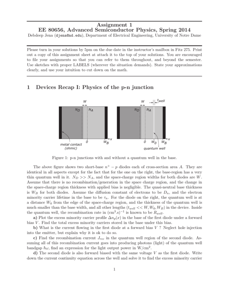
Assignment 1 EE 80656, Advanced Semiconductor Physics, Spring 2014 Debdeep Jena (djena@nd.edu), Department of Electrical Engineering, University of Notre Dame Please turn in your solutions by 5pm on the due date in the instructor’s mailbox in Fitz 275. Print out a copy of this assignment sheet at attach it to the top of your solutions. You are encouraged to file your assignments so that you can refer to them throughout, and beyond the semester. Use sketches with proper LABELS (wherever the situation demands). State your approximations clearly, and use your intuition to cut down on the math. 1 Devices Recap I: Physics of the p-n junction W ND metal contact (ohmic) NA 0 twell W ND WB x NA 0 W0 WB x quantum well Figure 1: p-n junctions with and without a quantum well in the base. The above figure shows two short-base n+ − p diodes each of cross-section area A. They are identical in all aspects except for the fact that for the one on the right, the base-region has a very thin quantum well in it. ND >> NA , and the space-charge region widths for both diodes are W . Assume that there is no recombination/generation in the space charge region, and the change in the space-charge region thickness with applied bias is negligible. The quasi-neutral base thickness is WB for both diodes. Assume the diffusion constant of electrons to be Dn , and the electron minority carrier lifetime in the base to be τn . For the diode on the right, the quantum well is at a distance W0 from the edge of the space-charge region, and the thickness of the quantum well is much smaller than the base width, and all other lengths (twell << W, W0 , WB ) in the device. Inside the quantum well, the recombination rate in (cm3 .s)−1 is known to be Rwell . a) Plot the excess minority carrier profile ∆np (x) in the base of the first diode under a forward bias V . Find the total excess minority carriers stored in the base under this bias. b) What is the current flowing in the first diode at a forward bias V ? Neglect hole injection into the emitter, but explain why it is ok to do so. c) Find the recombination current Jrec in the quantum well region of the second diode. Assuming all of this recombination current goes into producing photons (light) of the quantum well bandgap h̄ω, find an expression for the light output power in W/cm2 . d) The second diode is also forward biased with the same voltage V as the first diode. Write down the current continuity equation across the well and solve it to find the excess minority carrier 1 density at the location of the quantum well ∆np (W0 ). e) Show that as the recombination rate Rwell increases, the excess minority carrier concentration in the well decreases. Plot the minority carrier profile ∆np (x) for the second diode and compare with the first. Use it to explain which diode will switch faster. f ) What is the current that flows in the second diode for the same bias? Is it larger or smaller than for the first diode? Explain why. g) If you were required to increase the current flowing in the second diode by moving the quantum well (changing W0 ), which way (left or right) would you move the well? Explain. 2 Devices Recap II: Physics of the MOSFET We discussed the compact model of a long-channel MOSFET in class, which reproduces the drain current Id as a function of the drain and source voltages Vgs and Vds . An advantage of the model is its ability to provide the on-state characteristics (the family I − V curves): Id vs Vds for Vgs > Vth , and the sub threshold characteristics for Vgs < Vth using a single unified formalism. Consider a typical Si (ni ∼ 1010 /cm3 , ǫs ∼ 11.7) long-channel n-MOSFET with Na = 1017 /cm3 , an effective inversion channel mobility µ ∼ 200 cm2 /V.s, a SiO2 gate oxide with tox = 10nm and ǫox = 3.9. Calculate and plot the T = 300 K family Id /W − Vds curves for various Vgs − Vth , and the transfer characteristics log(Id /W ) − Vgs for a low and a high Vds first for L = 2µm, and then for L = 0.2µm. Indicate the on-off switching of the MOSFET. Find the subthreshold slope and compare to the Boltzmann limit of 60 mV/decade. Comment on the effect of source-drain scaling. 3 Quantum-Mech Recap I: Solutions of the Schrodinger Equation Quantum mechanical states of definite energy for electrons assume a central importance in applications. Make a table of where your columns are 1) the electric potential V (x), 2) the definite energy wavefunctions in real space ψE (x), and 3) the energy eigenvalues En , for a) The completely free electron in 1D V (x) = 0 in −∞ ≤ x ≤ +∞, b) The ‘quasi’-free electron in 1D V (x) = 0 in a ‘circle’ of length L, c) The electron in a box with V (x) = 0 for 0 ≤ x ≤ L and V (x) = ∞ for x < 0 and x > L, d) The simple harmonic oscillator V (x) = 21 kx2 . 4 Quantum-Mech Recap II: Probability currents We derived the quantum-mechanical expression for the probability current density carried by a ‘particle’ represented by a wavefunction ψ in class to be the vector j= h̄ (ψ ⋆ ∇ψ − ψ∇ψ ⋆ ). 2ime (1) Apply it to the following cases: a) Show that the probability current of an electron in a box (Problem 2) is zero. b) Electrons sit in the nz state of a heterostructure 2D quantum well of length L in the z−direction and are free to move in an area S in the x − y directions. The energy bandstructure is characterized by an effective mass m⋆ . Show that the probability current density for state |ki = (kx , ky , knz ) is the following (provide an expression for knz and explain the result) j(kx , ky , knz ) = 2 h̄ [ (kx x̂ + ky ŷ)] sin2 (knz z). SL m⋆ 2 (2) 5 The ballistic FET The charge current density carried by electrons is obtained from the probability current density by simply multiplying the electron charge J(k) = qj(k), and summing over all occupied electron P states: J = k J(k)f (k). Apply it to the following cases: a) Show that the charge current carried by a ‘quasi’-free electron in state k with V (x) = 0 in qh̄k . Discuss this result in terms of the more classical expression for current 0 ≤ x ≤ L is J(k) = m eL density J = q × n × v with n the electron density and v the velocity. b) Electrons sit in a 2-dimensional electron gas (2DEG) at T = 0 K with an electron density ns in a material with bandstructure characterized by the effective mass m⋆ . The system is at equilibrium, and no voltages are applied. Find the component of the current density Jx flowing in any given direction x̂. Evaluate it numerically for a typical AlN/GaN heterostructure with ns ∼ 1013 /cm2 and m⋆ ∼ 0.2me . Show that the net current is of course zero when no voltages are applied. We derived the characteristics of a ballistic field-effect transistor in class. Read Natori’s paper and use the notes to c) Compare and contrast the Id − Vds and log(Id /W ) − Vgs curves of the ballistic MOSFET model with the long channel compact model of problem 2 for a Si MOSFET channel length of L = 0.2µm for identical oxide barrier thickness. Notice that the ballistic (or quantum) model of the MOSFET characteristics contains neither µ nor L, but Planck’s constant h̄ makes an explicit appearance. Plot the room-temperature Id − Vds and Id − Vgs characteristics of ballistic FETs made of d) A semiconductor with dispersion E(k) = h̄2 k2 /2m⋆ with m⋆ = 0.05 and m⋆ = 0.2. Compare and comment: the smaller effective mass represents a narrow-gap semiconductor (such as GaAs) and the larger effective mass represents a wide-bandgap semiconductor (such as GaN). Use a valleydegeneracy of gv = 1. q e) 2D graphene with dispersion E(k) = h̄vF k = h̄vF kx2 + ky2 with vF = 108 cm/s, gv = 2, and zero bandgap. 3
