An Improved Feedthrough Logic for Low Power and High Speed
advertisement

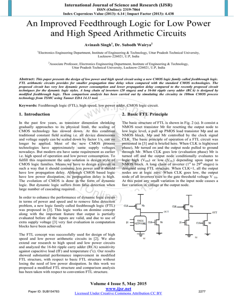
International Journal of Science and Research (IJSR) ISSN (Online): 2319-7064 Index Copernicus Value (2013): 6.14 | Impact Factor (2013): 4.438 An Improved Feedthrough Logic for Low Power and High Speed Arithmetic Circuits Avinash Singh1, Dr. Subodh Wairya2 1 Electronics Engineering Department, Institute of Engineering & Technology, Uttar Pradesh Technical University, Lucknow-226021, U.P, India 2 Associate Professor, Electronics Engineering Department, Institute of Engineering & Technology, Uttar Pradesh Technical University, Lucknow-226021, U.P, India Abstract: This paper presents the design of low power and high speed circuit using a new CMOS logic family called feedthrough logic. FTL arithmetic circuits provides for smaller propagation time delay when compared with the standard CMOS technologies. The proposed circuit has very low dynamic power consumption and lower propagation delay compared to the recently proposed circuit techniques for the dynamic logic styles. A long chain of inverters (20 stages) and a 16-bit ripple carry adder (RCA) is designed by modified feedthrough logic. Then comparison analysis has been carried out by simulating the circuitry in 180nm CMOS process technology from TSMC using Tanner EDA 14.11 tool. Keywords: Feedthrough logic (FTL), high speed, low power adder, CMOS logic circuit. 1. Introduction 2. Basic FTL Principle In the past few years, as transistor dimension shrinking gradually approaches to its physical limit, the scaling of CMOS technology has slowed down. At this condition traditional constant field scaling i.e. all device dimensions and voltage supply can be scaled down by factor 1/s, can no longer be applied. Most of the new CMOS process technologies have approximately same supply voltages nowadays. But modern era have same requirement as earlier i.e. high speed of operation and low power consumption. To fulfill this requirement the only solution is design style of CMOS logic families. Means we have to design a circuit in such a way that it should consume less power and it should have low propagation delay. Although CMOS based logic have low power dissipation, its propagation delay is high. The evolution of CMOS is done in the form of dynamic logic. But dynamic logic suffers from false detection when large number of cascading required. The basic structure of FTL is shown in Fig. 2 (a). It consist a NMOS reset transistor Mr for resetting the output node to low logic level, a pull up PMOS load transistor Mp and an NMOS block. Mp and Mr controlled by the clock signal CLK. The basic principle of operation of a FTL circuit was presented in [3] and is briefed here. When CLK is high(reset phase), Mr turned on and the output node pulled to ground through Mr. When CLK goes low (evaluation phase) Mr is turned off and the output node conditionally evaluates to logic high (VOH) or low (VOL) depending upon input to NMOS block. A long chain of inverter (1st to 29th stages) is designed using FTL structure. When CLK=1, all the output nodes are at logic zero. When CLK goes low, the output node of all inverters rises to the gate threshold voltage V TH. At this point any small variation in the input node causes a fast variation in voltage at the output node. In order to enhance the performance of dynamic logic circuit in terms of power and speed and to remove false detection problem, a new logic family called feedthrough logic (FTL) was proposed in [3]. This logic works on domino concept along with the important feature that output is partially evaluated before all the inputs are valid, and due to use of extra supply voltage [3] very fast evaluation in computation blocks have been achieved. The FTL concept was successfully used for design of high speed and low power arithmetic circuits in [2]. We also extend our research to high speed and low power circuits and analyzed the 16-bit ripple carry adder (RCA) sensitivity against capacitive load (fF) and temperature (oc). Our results showed substantial performance improvement in modified FTL structure, with respect to basic FTL structure without losing the need of low power dissipation. In this work we proposed a modified FTL structure and comparison analysis has been taken with respect to convention FTL structure. Paper ID: SUB154783 Volume 4 Issue 5, May 2015 www.ijsr.net Licensed Under Creative Commons Attribution CC BY 2277 International Journal of Science and Research (IJSR) ISSN (Online): 2319-7064 Index Copernicus Value (2013): 6.14 | Impact Factor (2013): 4.438 Figure 2: (a) Basic FTL structure, (b) Inverter using basic FTL, (c) Output waveform of 1st to 29th inverter stages 3. Proposed Modified FTL The proposed modified circuit is presented in fig.3 This circuit reduces VOL by using additional PMOS transistor M2 in series with M1, and NMOS transistors M3 and M4 prevents switching current through NMOS block . The operation of this circuit is similar to that of FTL in [3]. During reset phase i.e. when CLK = 1, output node is pulled to VDD/2 through M5, when CLK goes low (evaluation phase) M5 is turned off and the output node conditionally evaluates to logic high (VOH) or low (VOL) depending upon input to NMOS block. If the NMOS block evaluates to high then output node pulled toward VDD i.e. VOH =VDD, otherwise it goes at logic low i.e. VOL. The proposed FTL structure has been verified against basic FTL structure in [3] by designing a long chain of inverter consisting 20 stages. We have used 180nm CMOS process technology model file from TSMC at 250C. Power supply VDD is constant for all simulations and is equal to 1.8V. Circuits are simulated in Tanner EDA 14.11 tool. As The sufficient condition for equal propagation delay i.e. tplh =tphl in CMOS circuits as described in [1] may be given as:VT,n = VT,p ………………………(1) and, kn = kP (or Wp/Wn = µp/ µn) ………..(2) since electron mobility is greater than hole mobility (µn>µp) so we have used Wn /W p = 1.14 for all our simulations. Table I shows the dynamic power consumption, average values of propagation delays (tp), and power delay product comparison of proposed modified FTL and the existing FTL in [3] for 10 fF capacitive load at 100 MHz when simulation long chain of inverters (20 stages). The proposed FTL shows 48.7% less power consumption with a speed up factor of 1.32 with respect to existing FTL. Table 1: Simulation result for FTL and Modified FTL (20 stages of inverter) Logic Family Power Propagation delay PDP (µwatt) (nsec) (µwatt*nsec) FTL 887 0.795 705.17 Modified FTL 455 0.6027 274.23 5. 16-Bit Ripple Carry Adder Design and its Performance Analysis Fig.5.(a),and (b) shows basic sum and carry cell designed by proposed modified feedthrough logic. Simulation is done in 180nm technology at 25o C using Tanner EDA 14.11 Tool. Bar graph shows power dissipation, propagation delay and PDP of 16-bit RCA using modified FTL and existing FTL. Figure 3: Proposed Modified FTL structure 4. Performance Analysis of Proposed FTL Logic Paper ID: SUB154783 The Fig.5 (d),(e),(f) shows sensitivity of RCA designed by modified FTL against temperature(oC) and capacitance(fF). Bar graph Fig.5 (c) shows the 16-bit RCA performs fast logic evaluation (1.115 times) and consumes (46%) less power when simulated with proposed modified FTL structure as compare to existing FTL. The clock frequency and capacitive load is same as we have taken in inverter design. Volume 4 Issue 5, May 2015 www.ijsr.net Licensed Under Creative Commons Attribution CC BY 2278 International Journal of Science and Research (IJSR) ISSN (Online): 2319-7064 Index Copernicus Value (2013): 6.14 | Impact Factor (2013): 4.438 Figure 5: (a) Basic sum cell, (b) Basic carry cell, (c) Output comparison analysis of 16-bit RCA using basic FTL and proposed FTL,(d) Sensitivity of propagation delay against capacitive load, (e) sensitivity PDP against temperature variation, (f) sensitivity of power dissipation against capacitive load. The power delay product for both the structures is shown in Fig.5(c). We have obtained a sufficiently reduced value of power delay product; hence the performance of proposed modified structure is better than basic FTL structure. Fig. 5(d) shows effect of load capacitance variation on propagation delay. Our proposed structure has less sensitivity against increase in capacitive load than basic FTL structure. Fig.5 (e) shows effect of temperature variation on power delay product and Fig.5 (f) shows effect of load capacitance variation on dynamic power dissipation. 6. Conclusion and Future Scope In this paper, we proposed a low power and high speed dynamic circuit. The proposed circuit is simulated in 180nm CMOS process technology from TSMC using tanner EDA 14.11 tool. The proposed modified circuit when compared with recently modified circuits it consumes 46% less power without losing the need of high speed. The simulation for a long chain of inverter (20-stage) and 16-bit ripple carry adder is also carried out in this work. The simulation result Paper ID: SUB154783 confirms that for a given load and at same frequency of operation the power delay product of the proposed circuit is much better than that of existing FTL structure. The proposed circuit can be used for designing of low power and high speed processor where high speed and low power consumption is essential requirement. References [1] S. M. Kang, Y. Leblebici, „CMOS Digital Integrated Circuits: Analysis & Design‟, TATA McGraw- Hill Publication, 3e, 2003. [2] V. Navarro-Botello, J. A. Montiel-Nelson, and S. Nooshabadi,“ Low power and high performance arithmetic circuits in feedthrough CMOS logic family for low power application,” ASP J. Low power Electronics, vol. 2, no.2, Aug. 2006, pp. 300-307. [3] V. Navarro-Botello, J. A. Montiel-Nelson, and S. Nooshabadi, “Performance Analysis of high performance fast feedthrough logic families in CMOS,” IEEE Trans. Cir. & syst. II, vol. 54, no. 6, Jun. 2007, pp. 489-493. Volume 4 Issue 5, May 2015 www.ijsr.net Licensed Under Creative Commons Attribution CC BY 2279 International Journal of Science and Research (IJSR) ISSN (Online): 2319-7064 Index Copernicus Value (2013): 6.14 | Impact Factor (2013): 4.438 [4] S. Nooshabadi and J. A. Montiel-Nelson, “Fast feedthrough logic: A high performance logic family for GaAs,” IEEE Trans. Circuit Syst. I, Reg. Paper, vol. 51, no. 11, Nov.2004, pp. 2189-2203. [5] K.S. Yeo, K. Roy, „Low- Voltage, Low-Power VLSI Subsystems‟. [6] S .Mathew, M. Anders, R. Krishnamurthy, S. Borkar, "A 4 GHz 130 nm address generation unit with 32-bit sparse-tree adder core," IEEE VLSI Circuits Symp. , Honolulu, Hi,jun 2002, pp. 126-127. [7] J.M. Rabaey, A. Chandrakasan, B. Nikolic, 'Digital Integrated Circuits: A Design perspective' 2e PrenticeHall, Upper saddle River, NJ, 2002. [8] N. Weste, K. Eshraghian, 'Principles of CMOS VLSI Design, A systems perspective', Addision Wesley MA,1988. [9] Jin-Fa Lin,‟ Low-Power Pulse-Triggered Flip-Flop Design Based on a Signal Feed-Through Scheme‟. IEEE Transactions VLSI systems, Nov.-2012, pp. 1-5. Author Profile Avinash Singh received his B-tech degree in Electronics & Communication Engineering from Maharana Pratap Engineering College affiliated to Uttar Pradesh Technical University, Lucknow, India and is currently working toward his M-Tech degree in Microelectronics Engineering with the research interest in reducing power consumption and enhancing speed of digital circuits, from Institute of Engineering and Technology, Lucknow Uttar Pradesh Dr. Subodh Wairya received B. Tech (1993), M.Tech and Ph.D (2012) from HBTI, Kanpur, Jadavpur University, Kolkata and MNNIT Allahbad, India, respectively. His Ph.D research work was oriented towards PERFORMANCE EVALUATION OF HIGH SPEED LOW POWER CMOS FULL ADDER CIRCUITS FOR LOW VOLTAGE VLSI DESIGN. Currently, he is an Associate Professor at IET, lucknow(from 6 May 1996Present).He has also served as Scientist “B” Adhoc (One Year) at DRDO, Lucknow during January, 1995-January, 1996 and Graduate Engineer under Consultancy Project at HAL, Lucknow during From January, 1994- January, 1995 (one year). Also he is one of the authors of a book entitled “A Simplified Approach to Telecommunication and Electronic Switching Systems” by C.B.L. Srivastava, Neelam Srivastava & Subodh Wairya Published by Dhanpat Rai and Company in the year 2006. Paper ID: SUB154783 Volume 4 Issue 5, May 2015 www.ijsr.net Licensed Under Creative Commons Attribution CC BY 2280


