Design of 1 V Operating Fully Differential OTA Using NMOS Inverters
advertisement

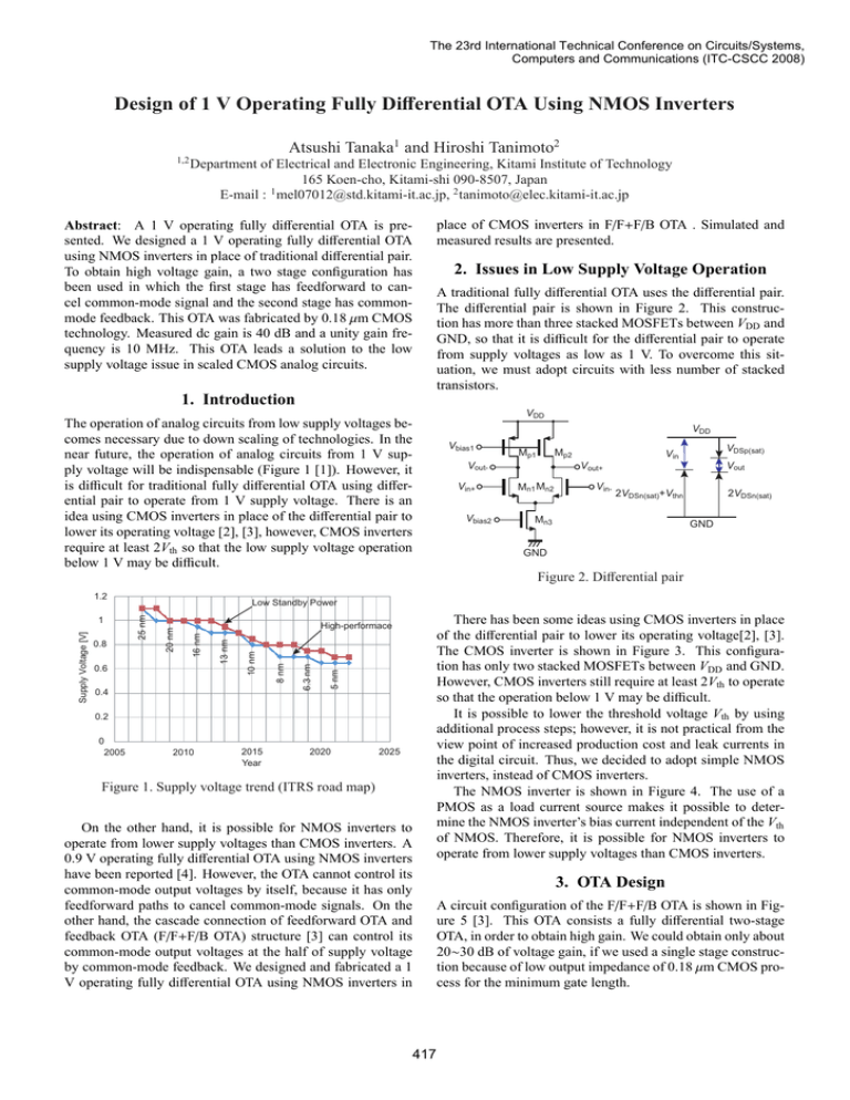
The 23rd International Technical Conference on Circuits/Systems, Computers and Communications (ITC-CSCC 2008) Design of 1 V Operating Fully Differential OTA Using NMOS Inverters Atsushi Tanaka1 and Hiroshi Tanimoto2 1,2 Department of Electrical and Electronic Engineering, Kitami Institute of Technology 165 Koen-cho, Kitami-shi 090-8507, Japan E-mail : 1 mel07012@std.kitami-it.ac.jp, 2 tanimoto@elec.kitami-it.ac.jp place of CMOS inverters in F/F+F/B OTA . Simulated and measured results are presented. Abstract: A 1 V operating fully differential OTA is presented. We designed a 1 V operating fully differential OTA using NMOS inverters in place of traditional differential pair. To obtain high voltage gain, a two stage configuration has been used in which the first stage has feedforward to cancel common-mode signal and the second stage has commonmode feedback. This OTA was fabricated by 0.18 μm CMOS technology. Measured dc gain is 40 dB and a unity gain frequency is 10 MHz. This OTA leads a solution to the low supply voltage issue in scaled CMOS analog circuits. 2. Issues in Low Supply Voltage Operation A traditional fully differential OTA uses the differential pair. The differential pair is shown in Figure 2. This construction has more than three stacked MOSFETs between VDD and GND, so that it is difficult for the differential pair to operate from supply voltages as low as 1 V. To overcome this situation, we must adopt circuits with less number of stacked transistors. 1. Introduction VDD The operation of analog circuits from low supply voltages becomes necessary due to down scaling of technologies. In the near future, the operation of analog circuits from 1 V supply voltage will be indispensable (Figure 1 [1]). However, it is difficult for traditional fully differential OTA using differential pair to operate from 1 V supply voltage. There is an idea using CMOS inverters in place of the differential pair to lower its operating voltage [2], [3], however, CMOS inverters require at least 2Vth so that the low supply voltage operation below 1 V may be difficult. VDD Vbias1 Mp1 Vin+ Vbias2 Vout+ Mn1 Mn2 Vin- VDSp(sat) Vin Mp2 Vout- Vout 2VDSn(sat) 2VDSn(sat)+Vthn Mn3 GND GND Figure 2. Differential pair 1.2 There has been some ideas using CMOS inverters in place of the differential pair to lower its operating voltage[2], [3]. The CMOS inverter is shown in Figure 3. This configuration has only two stacked MOSFETs between VDD and GND. However, CMOS inverters still require at least 2Vth to operate so that the operation below 1 V may be difficult. It is possible to lower the threshold voltage Vth by using additional process steps; however, it is not practical from the view point of increased production cost and leak currents in the digital circuit. Thus, we decided to adopt simple NMOS inverters, instead of CMOS inverters. The NMOS inverter is shown in Figure 4. The use of a PMOS as a load current source makes it possible to determine the NMOS inverter’s bias current independent of the Vth of NMOS. Therefore, it is possible for NMOS inverters to operate from lower supply voltages than CMOS inverters. 5 nm 6.3 nm 0.4 8 nm 10 nm 0.6 13 nm High-performace 16 nm 20 nm 0.8 25 nm Supply Voltage [V] 1 Low Standby Power 0.2 0 2005 2010 2015 Year 2020 2025 Figure 1. Supply voltage trend (ITRS road map) On the other hand, it is possible for NMOS inverters to operate from lower supply voltages than CMOS inverters. A 0.9 V operating fully differential OTA using NMOS inverters have been reported [4]. However, the OTA cannot control its common-mode output voltages by itself, because it has only feedforward paths to cancel common-mode signals. On the other hand, the cascade connection of feedforward OTA and feedback OTA (F/F+F/B OTA) structure [3] can control its common-mode output voltages at the half of supply voltage by common-mode feedback. We designed and fabricated a 1 V operating fully differential OTA using NMOS inverters in 3. OTA Design A circuit configuration of the F/F+F/B OTA is shown in Figure 5 [3]. This OTA consists a fully differential two-stage OTA, in order to obtain high gain. We could obtain only about 20∼30 dB of voltage gain, if we used a single stage construction because of low output impedance of 0.18 μm CMOS process for the minimum gate length. 417 VDD VDD VDSp(sat) VDSp(sat)+Vthp Mp Vout Vin Mn C-INV1 Vin −OUT C-INV2 C-INV3 C-INV4 C-INV12 C-INV11 C-INV10 C-INV5 C-INV6 C-INV7 C-INV15 C-INV14 C-INV13 Vout VDSn(sat)+Vthn VDSn(sat) +OUT −IN Figure 5. Configuration of F/F + F/B OTA Figure 3. CMOS inverter (C-INV) VDD C-INV1 VDD C-INV2 Mn GND VDSn(sat)+Vthn C-INV4 C-INV12 C-INV7 C-INV15 C-INV5 C-INV10 1/2gm 1/2gm Vout Vout Vin −OUT Vin Mp C-INV9 +IN VDSp(sat) Vbias C-INV16 C-INV8 GND GND C-INV9 +IN C-INV13 +OUT −IN VDSn(sat) C-INV16 C-INV8 GND (a) N-INV1 N-INV9 +IN Figure 4. NMOS inverter (N-INV) −OUT N-INV2 N-INV4 N-INV12 N-INV7 N-INV15 1/2gm 1/2gm To suppress common-mode gain, this OTA has feedforward paths and feedback paths. The first stage has feedforward paths for common-mode cancellation, while the second stage has common-mode feedback paths to stabilize the output common-mode voltage. The input common-mode voltage is detected by averaging two inverted inputs, and only the inverted common-mode voltage is fedforward via two replica inverters (C-INV4, C-INV7) to the inverters in main signal paths (C-INV1, C-INV8). Likewise, the output commonmode voltage is also detected by averaging two inverted outputs, and only the inverted common-mode voltage is fedback via two replica inverters (C-INV12, C-INV15) to the inverters in main signal paths (C-INV9, C-INV16). Hence, the differential-mode signals are not fedforward or fedback because of the averaging. This is shown in Figure 6 (a). Our main idea is to replace the CMOS inverters with NMOS inverters; however, simple replacements cause a problem. In the averaging stages, differential signal may not cancel out due to its class-A operation of the NMOS inverters. This is shown Figure 6 (b). This causes the differentialmode output to clip in its upper half portion, because some of the differential-mode component is fedback and lowers the differential-mode gain. This never occur if we use CMOS inverters. To solve this problem, we decline to use the NMOS inverters to average in the F/F OTA and F/B OTA stages. The proposed OTA is shown in Figure 7. First, we decline to use averaging action at the F/F OTA stage by disconnecting the outputs of N-INV3 and N-INV6. This permits signals to feedforward both common-mode and differential-mode; however, only the common-mode signals are canceled and the differential-mode signals aid due to the N-INV5 N-INV10 N-INV13 +OUT −IN N-INV8 N-INV16 (b) = 1/gm Figure 6. The flow of the differential signal of F/F+F/B OTA using CMOS inverters (a), and using NMOS inverters (b). cross connection around the feedforward paths. Second, in the F/B OTA stage, we adopted a resistive averaging circuit in front of the feedback circuit consisting of NMOS inverters (N-INV10∼13). This eliminates the differential-mode signals input to the feedback circuit, and only the common-mode feedback remains. The resistance of the averaging circuit must be large in order to keep the voltage gain high. In this design R = 220 kΩ is used, because the estimated output resistance of N-INV9(N-INV-14) is 22 kΩ. We assume a 0.18 μm CMOS process in the design. The gate length L of the NMOS inverters are 0.18 μm (minimum dimension) considering speed and power dissipation. Gate widths of the NMOS are designed to be 1.5 μm, and those of PMOS are designed to be 6 μm. The first stage inverters have all the same aspect ratio to keep common-mode cancellation high. In the second stage, main forward path inverters (NINV9, N-INV14) have ten times the larger gate width than the first stage inverters, because they must provide larger output currents. Other inverters are the same dimension as that of 418 Cc N-INV1 Rc The common-mode phase response could not be measured. Measurements for common-mode signal is difficult because the common-mode signal is very small due to a very large common-mode rejection ratio of the proposed OTA. However, because the measured common-mode gain is less than unity for all frequency range, a stability problem will not occur. Anyway, the measured results indicate its usefulness of the proposed circuit configuration operating at very low power supply voltage situations. N-INV9 +IN −OUT N-INV2 N-INV3 N-INV4 N-INV12 R N-INV11 N-INV5 N-INV6 N-INV7 N-INV10 R N-INV13 +OUT −IN N-INV8 N-INV14 Cc Rc 60 Figure 7. Proposed OTA Measured 40 Differential-mode 20 Gain [dB] the first stage. Each unit inverter consumes about 5 μA, and the output stage inverters consume about 50 μA from 1.0 V power supply. Total current consumption is about 170 μA. Because the proposed circuit is a two-stage amplifier, we introduced a conventional Miller compensation at the second stage as shown in Figure 7. The compensation capacitor Cc is 2 pF, and resistor Rc of 1 kΩ is put in series, in order to obtain phase margin of about 60 degrees. Simulated differentialmode gain is 44 dB, and the unity gain frequency is 13 MHz for no-load. 0 Simulated −20 −40 Common-mode −60 10 k 1M 100 k 10 M Frequency [Hz] 180 Measured Differential-mode Phase [deg.] 4. Simulated and Measured Results The proposed OTA was designed and fabricated by using TSMC 0.18 μm 1P6M mixed signal CMOS technology. A micrograph of the fabricated OTA is shown in Figure 8. The size of the fabricated OTA is 315.5 μm × 193.8 μm. The large area of the right side is occupied by resistors of the averaging circuit (2 × 220 kΩ). 90 0 Simulated 10 k 100 k 1M Frequency [Hz] 10 M 193.8 m Figure 9. Bode plot of the proposed OTA Figure 10 (a) shows measured output clipping levels to show the maximum output voltage swings of the two outputs. Each output voltage swings 880 mVp-p at 1 V power supply, as expected from the simulation result. Figure 10 (b) shows the maximum differential output voltage swing, which is 1.8 Vp-p at 1 V power supply. It has been confirmed that the proposed OTA has a very large output swing capability even in a low power supply voltage. The simulated and measured performances of the proposed OTA are summarized in Table 1. Unfortunately, its current consumption was not measured, because the power supply line is common to other circuits on the same chip. 315.5 m Figure 8. Chip micrograph of the proposed OTA Figure 9 shows the simulated and measured frequency responses of the proposed OTA. The simulated differentialmode gain is 42 dB and the measured gain is 39 dB for a 100 kΩ load with a 13 pF capacitor in parallel. For commonmode, the simulated gain is −33 dB and the measured gain is −35 dB for the same condition. These results indicate that the measured responses of the differential-mode are well matched with the designed responses. 5. Conclusion We proposed an NMOS inverter based fully differential twostage OTA, which can operate from 1 V power supply. The proposed OTA has been designed and fabricated in 0.18 μm CMOS process. The measured results confirm that the OTA can successfully operate from 1 V power supply with about 40 dB, unity gain bandwidth of about 10 MHz at 170 μA of 419 Acknowledgments The authors thank Dr. H. Yanagisawa of Kitami Institute of Technology, for his support in preparing CAD tools. This work is partly supported by VLSI Design and Education Center (VDEC), the University of Tokyo in collaboration with Cadence Design Systems, Inc. 880 mVp-p References [1] ITRS, “International Technology Roadmap for Semiconductors 2007 Edition Process Integration, Devices & Structures,” http://www.itrs.net/Links/2007ITRS/2007 Chapters/2007 PIDS.pdf, April, 2008. [2] Bram Nauta, “A CMOS transconductance-C filter technique for very high frequencies,” IEEE J. Solid-State Circuits, Vol. 27, pp. 142–153, February, 1992. [3] Keishi Komoriyama, Eiichi Yoshida, Makoto Yashiki, Hiroshi Tanimoto, “A Very Wideband Fully Balanced Active RC Polyphase Filter Based on CMOS Inverters in 0.18 μm CMOS Technology,” Symposium on VLSI Circuits Dig. Tech. Pap., pp. 98–99, June, 2007. [4] Takeshi UENO, Tetsuro ITAKURA, “A 0.9 V 1.5 mW Continuous-Time ΔΣ Modulator for W-CDMA,” IEICE Trans. Fundamentals, Vol.E88-A, No.2, pp 416–468, February, 2005. [5] Behzad Razavi, Design of Analog CMOS Integrated Circuits, McGraw-Hill, New York, 2001. (a) 1.8 Vp-p (b) Figure 10. Measured output swing of the proposed OTA. Two single-end output voltages (a), and differential output voltage (b). Table 1. Performance summary of the proposed OTA (RL =100 kΩ, CL =13 pF) Item Simulated Measured Supply voltage 1.0 V 1.0 V Current consumption 170 μA − Open-loop dc gain 42 dB 39 dB Unity gain frequency 9 MHz 10 MHz Phase margin 52 deg. 53 deg. Output voltage swing (28∼974) mV (50∼ 930) mV CMRR @10 kHz 75 dB 74 dB current consumption. This OTA provides a solution to the low supply voltage issue in scaled CMOS analog circuits. The differential-mode gain of the proposed OTA is lower compared with that of reference [3] in this design; however, we can improve its gain by using larger gate lengths. The proposed OTA can operate from lower supply voltage than the reference [3], and has better control over current consumption because it is based on class A inverters unlike class AB CMOS inverters in the reference [3]. The proposed OTA may be applied to integrated variable filters because its transconductance can be controlled by changing its operating current. 420


