Application Note
Understanding
Digital Video
Interface (DVI)
Compliance Testing
Engineers involved in design, characterization and validation of DVI
devices face daily pressure to speed new products to marketplace. The
challenge for these designers is to have their devices be inter-operable
with a huge set of DVI devices from other companies, already available
in the market place. Successfully validating their designs to the DVI
specification by performing compliance testing ensures the designer of
a robust design.
Digital Visual Interface (DVI) is a display interface that supports
data transfer from a PC to a flat panel display in digital format.
Used extensively in the PC market, DVI eliminates the need to
convert this digital data into analog data for transmission,
improving performance and video quality.
The DVI specification and the DVI Test and Measurement Guide
introduce new testing requirements. As a DVI device designer
you must properly characterize designs and verify compliance
to ensure inter-operatability among other DVI devices. This is
necessary for a pleasant user experience.
1
www.tektronix.com/oscilloscopes
An appropriate tool set is critical for performing DVI physical layer
tests as specified by the DVI Test and Measurement Guide.
This application note will focus on understanding and performing
physical layer measurements.
Understanding Digital Video Interface (DVI) Compliance Testing
Application Note
DVI Basics
DVI uses a high-speed serial interface that uses transition minimized
differential signaling (TMDS) to send data to the monitor. TMDS
conveys data by transitioning between “on” and “off” states. An
advanced encoding algorithm that uses Boolean exclusive OR
(XOR) or exclusive NOR (XNOR) operations is applied to minimize the
transitions. Minimizing transitions avoids excessive electromagnetic
interference (EMI) levels on the cable. An additional operation is
performed to balance the DC signal.
Figure 1 shows the flow of display (or pixel) data from the graphics
controller through TMDS mechanisms (implemented in a chip on the
graphics card or in the graphics chip set) and the display controller.
In this process, incoming 8-bit data is encoded into 10-bit transitionminimized, DC-balanced characters. (The first eight bits are the
encoded data; the ninth bit identifies whether the data was encoded
with XOR or XNOR logic; the tenth bit is used for DC balancing.)
As shown in Figure 1, DVI allows for up to two TMDS links. Each
link is composed of three data channels for RGB information and
has a maximum bandwidth of 165 MHz, which equates to 165
million pixels per second. For a dual link implementation, this
becomes 330 million pixels per second. The two links share the
same clock so that bandwidth can be divided evenly between them.
The system enables one or both links, depending on the capabilities
of the monitor.
Signal Speeds at PHY Layer
165 MHz is the fastest clock speed that DVI can encounter.
However, data is transmitted 10 times faster than the clock. Hence,
DVI can encounter data rates up to 1.65 Gbps. This translates to the
fastest rise times of 75ps on the highest DVI resolutions. Current
implementations have typical rise times of the order of 250 ps to
300 ps.
Display Resolutions
Video Electronics and Electronics Association (VESA) maintains a
set of standard display resolutions. Table below reviews some of
the standard PC display resolutions.
2
www.tektronix.com/oscilloscopes
Source: Digital Visual Interface specification, revision 1.0, 4/2/99,
Digital Display Working Group
Figure 1. TMDS Logical Links.
Resolution Name
Pixel Resolution
Video Graphics Array (VGA)
640 x 480
Super VGA (SVGA)
800 x 600
Extended Graphics Array (XGA)
1024 x 768
Super XGA (SXGA)
1280 x 1024
Ultra XGA (UXGA)
1600 x 1200
High-Definition TV (HDTV)
1920 x 1080
Quad XGA (QXGA)
2048 x 1536
Many DVI devices support proprietary non-standard resolutions also.
However, physical layer testing for these proprietary resolutions
essentially remains similar in terms of the test methodology and the
tests to be performed.
Understanding Digital Video Interface (DVI) Compliance Testing
Application Note
DVI Compliance Testing
DVI specification requires developers to comply with several
stringent compliance tests for DVI designs. This is because there
are hundreds of DVI devices and these devices must conform to
Digital Display Working Group (DDWG) furnished specifications.
This is necessary for devices to interoperate, which is essential
for a satisfactory user experience and for the mass adoption of
DVI technology.
Developers are required to self-comply by performing tests as per
the DVI Test and Measurement Guide. This is applicable for all
DVI devices.
Compliance testing is conducted for transmitter, cable and receiver
at various test points as shown in the Figure 2. These test points
are defined to be the contact point between the mated connected
pairs of the cable assembly
Test fixture or breakout boards are required to probe the various
test points (TP2 and TP3).
DVI Electrical Tests
Signal Integrity Testing
Since DVI designs can encounter typical rise times of the order of
250 ps, signal integrity testing is of paramount importance. Various
tests that need to be conducted to verify signal integrity are:
Figure 2.
Eye Diagram Test Methodology
The DVI specification calls for guaranteeing 10^-9 pixel error rate.
To achieve this 1 billion acquisitions on the oscilloscope is not
practical. An alternate approach is to acquire less number of
acquisitions and then use the statistical six-sigma method to infer
a Pass or a Fail. But there are issues with the six-sigma statistical
approach as it assumes the distribution to be gaussian, whereas the
actual distribution is not gaussian due to systematic jitter.
Hence, the DVI test methodology, for a psuedo random pattern
recommends gathering one million acquisitions to ensure simulation
of worst-case jitter conditions. This is a more practical method and
is recommended by the test and measurement guide as Method II.
So, after calculating the Tbit and Vswing is determined, both these
parameters are used to construct the eye mask.
— Eye diagram test
The DVI Test and Measurement Guide recommends recovering the
clock (single ended) from the transmitter (differential) clock and use
this recovered clock as a trigger source to the oscilloscope for testing.
— Jitter testing
The Challenge
— Skew testing
Compliance testing is a challenge if it needs human intervention.
The human intervention makes testing difficult and slows the test
process. The DVI transmitter eye-masks (TP2) are normalized and
change dynamically with the Vswing and Tbit values, while the cable
and receiver masks (TP3) are normalized in time and change
according to the changes in Tbit value of the signal. This makes
manual testing subjective and error prone.
— Rise time
— Fall time
Conducting Signal Integrity Testing
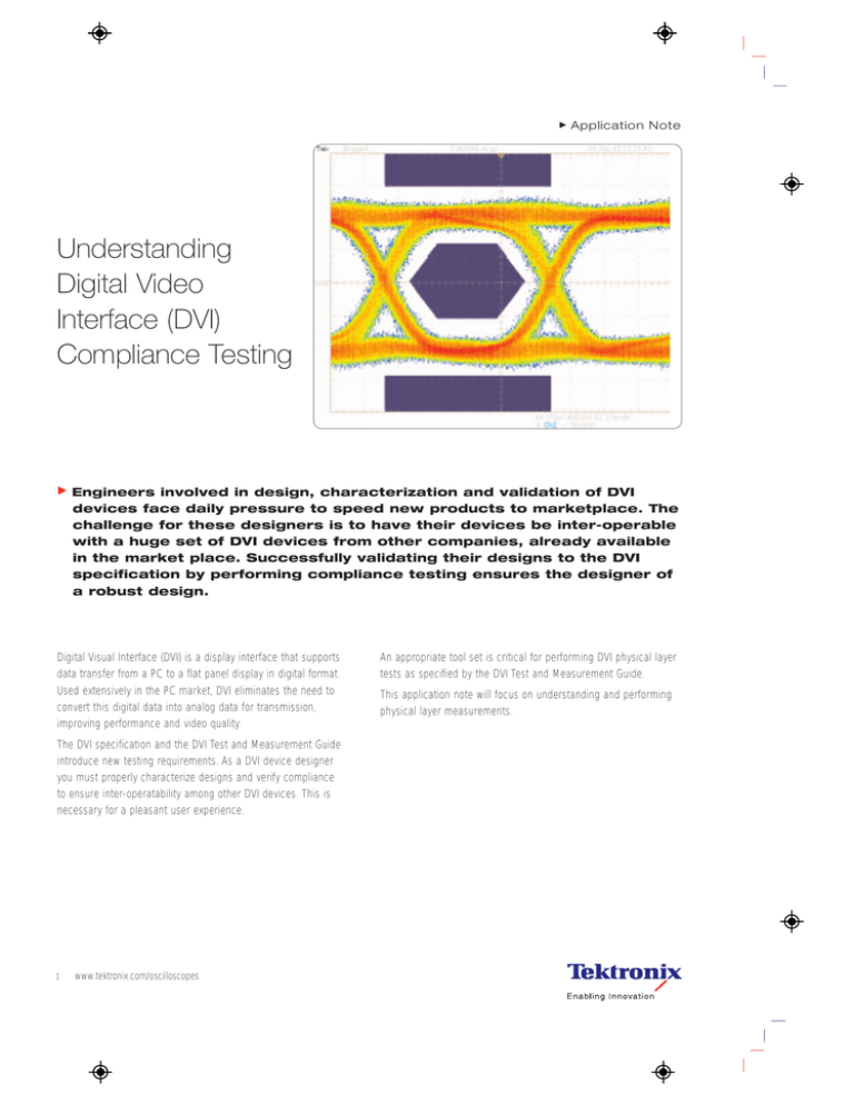
Eye diagram testing is the most critical of all the signal integrity
tests. The eye diagram test provides information about jitter,
amplitude and ringing effects on the signal. A pass in the eye
diagram test assures a robust design.
Tbit Calculation – Essential Prerequisite to Testing
One unit interval of the DVI signal is referred to as Tbit. The DVI
Test and Measurement guide recommends Tbit calculation to be
performed on the transmitter (differential) clock.
Further, there are 10 data bits in one clock bit (pixel) and designers
sometimes may be interested to test all the 10 data bits. In such a
case, one needs to figure out the worst data bit which is essentially
the data bit with the smallest Tbit value amongst the 10 data bits.
www.tektronix.com/oscilloscopes
3
Understanding Digital Video Interface (DVI) Compliance Testing
Application Note
Test Equipment
Signal integrity testing requires a real-time oscilloscope such as the
TDS7704B, TDS7404B or CSA7404B digital phosphor oscilloscopes
(DPO) and differential probes such as the P7330 or P7350 probes.
In addition, this testing requires automated software such as TDSDVI
and a test fixture.
Figure 3, shows the TDSDVI compliance test software on a TDS7404
DPO. This test package fully automates the signal integrity test
process, allowing designers to perform quick, easy and reliable tests
on their designs.
A user must perform Tbit calculation for the device under test (DUT).
Then select the measurements to be performed on a transmitter,
cable or the receiver. The application must then be configured as
shown in Figure 4. After completing these steps the user can run
the application to get the test results.
Figure 3.
The test software eliminates the tedium of manual, time-consuming
oscilloscope set-ups, cursor placements for Tbit and Vswing calculation,
and creating the mask by manually using the Tbit and Vswing values to
calculate the mask coordinates and finally comparing the actual
results with the DVI specification to ascertain a pass or a fail. The
results are automatically displayed as illustrated in Figure 5.
Automated testing based on objective pass/fail detection without
human intervention helps to achieve the time-to-market goals. The
results are obtained quickly and are more reliable.
Figure 4.
TDSDVI test software dramatically enhances productivity.
Selecting Tools for DVI Physical Layer Testing
A good set of tools is the key to dependable, repeatable and
reliable testing. System bandwidth and rise-time are the obvious
considerations when choosing a compliance test solution.
Oscilloscope
An oscilloscope is the most crucial test instrument for DVI
measurements. When selecting an oscilloscope for these
measurements it is important to consider the oscilloscope’s
bandwidth, rise time, and the acquisition technology.
Bandwidth and Rise-time
DVI specification defines rise-time from 20% - 80%. This is the
rise-time of the differential signal as it transitions from 20% to 80%
of its differential amplitude. It is important to make sure that the
oscilloscope can handle rise-times of the given order. The required
rise-time of the oscilloscope should be at least three times faster
than that of the signal rise-time. DVI typically (up to UXGA) encounters
rise-times of the order of 250 ps to 300 ps. Hence, an oscilloscope
4
www.tektronix.com/oscilloscopes
Figure 5.
with a rise-time of about 50 ps to 100 ps is the best tool for DVI
conformance testing. The TDS7704B and TDS7404B oscilloscopes
offer bandwidths of 7 GHz and 4 GHz with rise times (20% - 80%)
of 43 ps and 72 ps, respectively.
Understanding Digital Video Interface (DVI) Compliance Testing
Application Note
Acquisition Speed
DVI specification for eye testing recommends acquiring a million
acquisitions for creating the worst-case jitter condition in the eye
diagram. Using a digital storage oscilloscope might take the user
about an hour to accumulate one million acquisitions. A Digital
Phosphor Oscilloscope (DPO) in FastAcq mode acquires a million
acquisitions in less than 10 seconds and hence allows performing
compliance testing quickly. TDS7704B, TDS/CSA7404B Digital
Phosphor Oscilloscopes offer acquisition speeds up to 400,000
waveforms per second and hence quicken the entire test
Probes
Since the DVI signals are differential in nature, a differential probe
is extremely important. Using pseudo-differential methods of
channel subtraction result in unreliable measurements.
Figure 6. DDWG furnished TPA-P fixture.
The recommended probes for DVI testing are P7350, P7330 or
P6330.
Test Software
Compliance testing is a challenge if it needs human intervention.
Human intervention makes testing difficult and slows the test
process. The DVI transmitter eye-masks (TP2) are normalized and
change dynamically with the Vswing and Tbit values, while the cable
and receiver masks (TP3) are normalized in time and change
according to the changes in Tbit value of the signal. Further, a user
may have to locate the worst eye opening among the ten data bits.
This makes manual testing subjective and error prone.
TDSDVI software is the industry’s first tool set to enable engineers
to perform reliable in-house compliance testing to the DVI specification.
It offers a comprehensive range of tests for transmitter, cable
and receiver testing for complete standards validation. Automatic
“one-button” operation ensures faster testing with higher reliability,
in conformance with the DVI Test and Measurement Guide.
Figure 7. DVI TPA-R TDR fixture.
Tektronix fixtures:
DVI TPA-R Test adapter set – 013-A014-50 Includes:
2) DVI TPA-R TDR
Test Fixtures
1) DVI TPA– R DI (differential)
The test fixture is a crucial component that enables probing for
every test set up. Also, the DVI test and measurement guide
recommends recovering the clock (single ended) from the transmitter
(differential) clock and use this recovered clock as a trigger source
to the oscilloscope for signal integrity testing. The ideal test fixture
should provide a PLL (Phased Locked Loop) in accordance to the
DVI specifications and also provide access to the differential data
lines for probing.
1) DVI TPA – R SE (single ended)
www.tektronix.com/oscilloscopes
5
Understanding Digital Video Interface (DVI) Compliance Testing
Application Note
Figure 8. Jitter setup menu in DTG5274.
Figure 9. Connecting an arbitrary waveform generator to increase range and
variety of jitter.
Receiver Jitter Tolerance and Receiver
Sensitivity Testing
Jitter Tolerance
‘Jitter Generation’
One of the most critical characteristics of a receiver is its tolerance
to specified levels of jitter in the transmitted clock signals. The
DTG5274 can generate jitter on the DVI clock signal for jitter values
of less than 1.56MHz without the need for external equipment
using a simple setup menu (see Figure 8). To test jitter tolerance at
frequencies above 1.56MHz, or to evaluate two elements of jitter
frequency, an AWG710 arbitrary waveform generator can be connected
to the DTG5274 as shown in Figure 9. The combination provides
jitter frequencies greater than 10MHz and multi frequency jitter
signals and defined with a simple equation editor Figure 8.
clock = 3.7125e9
‘ Sampling Clock
size = 148500
‘ Waveform Length
k00_ = 1e6
‘ Jitter Frequency 1
k01 = 10e6
‘ Jitter Frequency 2
k1
‘ Clock Frequency
= 74.25e6
k20 = 500e-12
‘ Jitter Amplitude 1
k21 = 500e-12
‘ Jitter Amplitude 2
k3
‘ Vertical Scale
=5
“output.wfm” =
k3 * sin(2 * pi * k1 * (time + k20/2 * sin(2 * pi * k00 * time)
+ k21/2 * sin(2 * pi * k01 * time) ))
“output.wfm”.marker1 = “marker.wfm”.marker1
‘ Clock for DTG5274
“output.wfm”.marker2 = “marker.wfm”.marker2
‘ Trigger for DTG5274
Figure 10. The equation file for AWG710 to generate jitter with two frequency elements.
6
www.tektronix.com/oscilloscopes
Understanding Digital Video Interface (DVI) Compliance Testing
Application Note
Receiver Sensitivity
Data signals are varied over a specified range of levels to test the
display equipment’s ability to tolerate reduced signal voltage. The
DTG5274 provides more quantitative and reproducible test results
than previous methods that used multiple length cables to attenuate
the signals. By providing continuous control of voltage levels in
multiple channels, the DTG5274 easily covers all levels within the
operating range of the receiver (and beyond) to allow a complete
sensitivity analysis. Figure 11 illustrates how easily the sensitivity
test signals can be set up in the DTG5274 using its graphic voltage
setup menu.
Figure 11. Voltage Level setup menu in DTG5274
Conclusion
.
DVI technology enables higher-end displays to move to digital-interface
designs hence improving the performance and video quality.
However, this switch from analog transmission to digital transmission
presents new challenges that the designer must resolve.
Tektronix offers a comprehensive tool set –sophisticated oscilloscopes,
high-speed data time generator, arbitrary waveform generators,
differential probes and ingenious test software to enable DVI
designers to perform quick, accurate and reliable compliance
testing and physical layer validation of their designs. Collectively,
this tool set provides superior performance and reliable in-house
compliance testing along with unmatched ease-of-use, making it
an ideal solution for DVI measurements.
www.tektronix.com/oscilloscopes
7
DPO – Digital Phosphor Technology
Contact Tektronix:
ASEAN / Australasia / Pakistan (65) 6356 3900
You have to see it to believe it.
A Digital Phosphor Oscilloscope (DPO) is ideal for those who
need the best design and troubleshooting tool for a wide
range of applications for communication mask testing, digital
debug of intermittent signals, repetitive digital design and
timing applications. Covering a spectrum of bandwidth from
100 MHz to 7 GHz, Tektronix offers a wide selection of DPOs
for you to see a world others don’t.
Austria +43 2236 8092 262
Belgium +32 (2) 715 89 70
Brazil & South America 55 (11) 3741-8360
Canada 1 (800) 661-5625
Central Europe & Greece +43 2236 8092 301
Denmark +45 44 850 700
Finland +358 (9) 4783 400
France & North Africa +33 (0) 1 69 86 80 34
Germany +49 (221) 94 77 400
Hong Kong (852) 2585-6688
India (91) 80-22275577
OpenChoice™
Italy +39 (02) 25086 1
Provides more choices for your networking
and analysis solutions.
OpenChoice is a collection of software libraries, utilities, samples,
industry-standard protocols and interfaces offered with many
Tektronix oscilloscopes and logic analyzers. From 60 MHz to 6 GHz,
OpenChoice allows you to communicate with your oscilloscope
or logic analyzer over a network, using numerous connectivity
protocols and physical interfaces, such as GPIB, Ethernet, RS-232
and shared memory.for you to see a world others don’t.
Japan 81 (3) 6714-3010
Mexico, Central America & Caribbean 52 (55) 56666-333
The Netherlands +31 (0) 23 569 5555
Norway +47 22 07 07 00
People’s Republic of China 86 (10) 6235 1230
Poland +48 (0) 22 521 53 40
Republic of Korea 82 (2) 528-5299
Russia, CIS & The Baltics +358 (9) 4783 400
South Africa +27 11 254 8360
Spain +34 (91) 372 6055
Sweden +46 8 477 6503/4
Taiwan 886 (2) 2722-9622
TekConnect®
Superior signal fidelity and unparalleled versatility
at your fingertips.
TekConnect interface takes probe intelligence to the next level
whether you are measuring high voltage, current, power, or
even micro-volt level signals. The TekConnect interface ensures
superior signal fidelity with useful bandpass up to 18 GHz at
the oscilloscope input, while offering unparalleled versatility.
With the TekConnect interface, you can be assured that
maximum signal integrity is maintained to meet your present
and future bandwidth needs.
Oscilloscope Software
Turn your general purpose oscilloscope
into a highly specialized analysis tool.
Tektronix offers exceptional application solutions that instill
your oscilloscope with specific technology or procedure
expertise, vastly simplifying the development and testing of
specialized designs. From serial data standards to power
measurements, Tektronix has the broadest selection of
oscilloscope software to convert your oscilloscope into a
highly specialized and power analysis tool.
8
8
www.tektronix.com/oscilloscopes
United Kingdom & Eire +44 (0) 1344 392400
USA 1 (800) 426-2200
USA (Export Sales) 1 (503) 627-1916
For other areas contact Tektronix, Inc. at: 1 (503) 627-7111
Updated 01 March 2004
For Further Information
Tektronix maintains a comprehensive, constantly expanding collection
of application notes, technical briefs and other resources to help
engineers working on the cutting edge of technology. Please visit
www.tektronix.com
Copyright © 2004, Tektronix, Inc. All rights reserved. Tektronix products are covered by U.S. and
foreign patents, issued and pending. Information in this publication supersedes that in all previously
published material. Specification and price change privileges reserved. TEKTRONIX and TEK
are registered trademarks of Tektronix, Inc. All other trade names referenced are the service marks,
trademarks or registered trademarks of their respective companies.
2/04 FLG/WWW
55W-17554-0
