Electron Devices Gain and Decibel (dB) dB Quick Table (20log10X)
advertisement

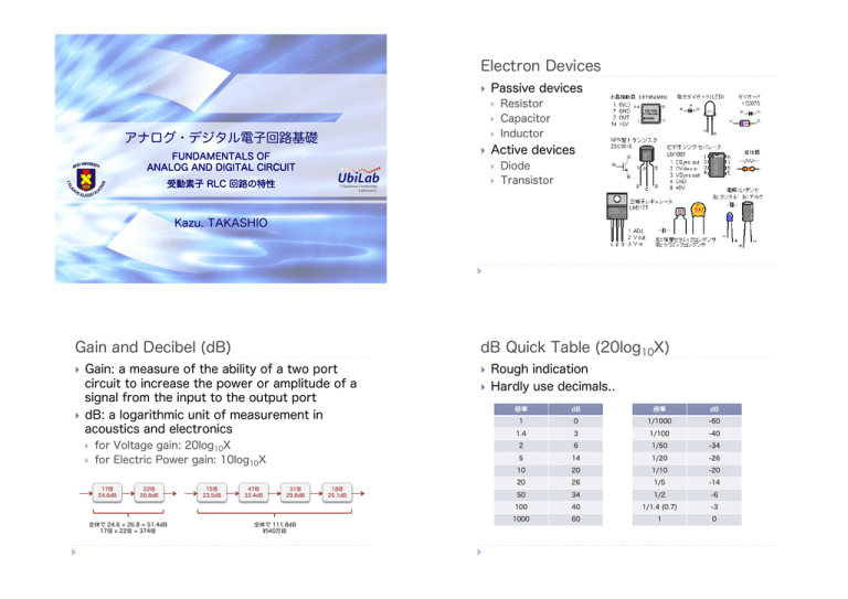
Electron Devices ! Passive devices ! ! アナログ・デジタル電子回路基礎 ! ! FUNDAMENTALS OF ANALOG AND DIGITAL CIRCUIT Active devices ! 受動素子 RLC 回路の特性 Resistor Capacitor Inductor ! Diode Transistor Kazu. TAKASHIO Gain and Decibel (dB) Gain: a measure of the ability of a two port circuit to increase the power or amplitude of a signal from the input to the output port ! dB: a logarithmic unit of measurement in acoustics and electronics ! ! ! for Voltage gain: 20log10X for Electric Power gain: 10log10X 17倍 24.6dB 22倍 26.8dB 全体で 24.6 + 26.8 = 51.4dB 17倍 x 22倍 = 374倍 15倍 23.5dB 47倍 33.4dB 31倍 29.8dB 全体で 111.8dB 約40万倍 18倍 25.1dB dB Quick Table (20log10X) ! ! Rough indication Hardly use decimals.. 倍率 dB 倍率 dB 1 0 1/1000 -60 1.4 3 1/100 -40 2 6 1/50 -34 5 14 1/20 -26 10 20 1/10 -20 20 26 1/5 -14 50 34 1/2 -6 100 40 1/1.4 (0.7) -3 1000 60 1 0 Resistor (r, R, RES) Passive two-terminal electrical component that implements electrical resistance.. ! Types ! ! ! ! Capacitor (Condenser, C) Passive two-terminal electrical component used to store energy electrostatically in an electric field.. ! Fixed resistor Potentiometer Trimmer ! ! ! Materials ! ! ! ! ! ! Carbon film resistor Solid resistor Metal film resistor Metal oxide film resistor Wirewound resistor Cement resistor Inductor (Coil, L) Passive two-terminal electrical component which resists changes in electric current passing through it.. ! ! Holding charge on its facing surfaces Reservoir temporally pooling and discharging Blocking DC, but passing AC (Capacitive Reactance) The more AC frequency is raised, the more the capacitive reactance goes down.. Passing DC, but resisting AC (Induced Reactance) The more AC frequency is raised, the more the induced reactance goes up.. Phase ! ! Phase: Position and distance between two wave signals Be shifted by the presence of impedance in an electric circuit signals pass through.. x 0 0 位相が x だけずれている (x だけ進んでいる) Impedance ! ! ! Impedance Resistance of a circuit depending of the frequency of an electric signal wave Represented as a complex quantity, where the real part is the resistance and the imaginary part is the reactance.. Z = R + jx ! ! ! ! ω = 2πf tanφ = x/R 2 コイル コンデンサ ! 虚数 j (リアクタンス) インピーダンス Z x コンデンサ ??? φ Simulation of a RLC Circuit Impedances of C1 and L1 are 1kΩ at 1kHz.. ! Capacitor 2 R ! Inductor コイル in an Inductor: jx = jωL in a Capacitor: jx = 1/jωC = -j/ωC R +x ! ! C1:(2π・1kHz・159nF)-1 L1:2π・1kHz・159mH 実数 r (抵抗) RLC Circuit: DC Analysis (DC Sweep) ! Simulation conditions ! ! MacOS X: Right click on the schematic > Draft > SPICE directive > Right click in the text field > Help me edit.. > Analysis Cmd. Win: Right click > Edit Simulation Cmd. RLC Circuit: AC Analysis ! RLC Circuit: AC Analysis Linear small-signal frequency domain analysis ! ! ! Analyzing variability over time (like an oscilloscope view).. ! ! ! Impedance ! ! Frequency axis: logarithmic [Octave, Decade],linear [Linear] RLC Circuit: Transient Analysis ! ! Output: Voltage gain and phase variation Analysis Cmd. (Win:Edit Simulation Cmd.) > AC Analysis AC power source: SIN(0 1 1kHz 0 0 0) Stop Time:3m,Time to Start ..: 0,Max Timestep Size:3u Impedances of R1, C1 and L1: ZR ZC ZL(1kΩ) ZC = 1 / (2π x f x C) ... V(l): Low-pass filter ZL = 2π x f x L ... V(c): Hi-pass filter RLC Circuit: Transient Analysis ! Detail analysis ! ! ! Voltage wave at R2:V(in) - V(c) ([Add Trace] icon) Add new graph: Menu > Add Plot Pane Why the V(c) getting 0.7 V(in) rather than the half of it? Exercise ! Simulate the resonance characteristic of the RLC circuit.. ! Exercise ! Step analysis: .step param Rv list 100 316 1k 1.41k 2k Fix the R1 to 100Ω and use sine-signal waves.. ! ! ! ! Discuss why the gain was increased 20dB at R1 = 100Ω? Submit to.. ! ! SFC-SFS Deadline.. ! ! ! Transient analysis: .trans 0 50m 0 5u Voltage between both ends of the L1: V(rl) - V(out) 9th Oct. 23:59 Hints.. ! Resonance frequency


