STLVDS385B
+ 3.3 V programmable LVDS transmitter 24-bit
flat panel display (FPD) link-85 MHz
Features
■
20 to 85 MHz shift clock support
■
Best-in-class set & hold times on Txinputs
■
Tx power consumption < 130 mW (typ) @85
MHz grayscale
■
Tx power-down mode < 200 µW (max)
■
Supports VGA, SVGA, XGA and single/dual
pixel SXGA.
)
s
t(
c
u
d
■
Narrow bus reduces cable size and cost
■
Up to 2.38 Gbps throughput
■
Up to 297.5 megabytes/sec. bandwidth
■
345 mV (typ) swing LVDS devices for low EMI
■
PLL requires no external components
■
Compatible with TIA/EIA -644 LVDS standard
e
t
e
)
s
t(
Description
c
u
d
l
o
s
P
e
et
l
o
s
Ob
)
s
t(
c
u
d
o
r
edge or falling edge strobe transmitter will inter
operate with a falling edge strobe receiver without
any translation logic.
b
O
-
l
o
bs
P
e
et
O
)
The STLVDS385B transmitter converts 28 bits of
LVCMOS/LVTTL data into four LVDS (low voltage
differential signaling) data streams. A phaselocked transmit clock is transmitted in parallel with
the data streams over a fifth LVDS link. Every
cycle of the transmit clock 28 bits of input data are
sampled and transmitted. At a transmit clock
frequency of 85 MHz, 24 bits of RGB data and 3
bits of LCD timing and control data (FPLINE,
FPFRAME, DRDY) are transmitted at a rate of
595 Mbps per LVDS data channel. Using a 85
MHz clock, the data throughput is 297.5
Mbytes/sec. The transmitter can be programmed
for rising edge strobe or falling edge strobe
through a dedicated pin. A rising
ro
o
r
P
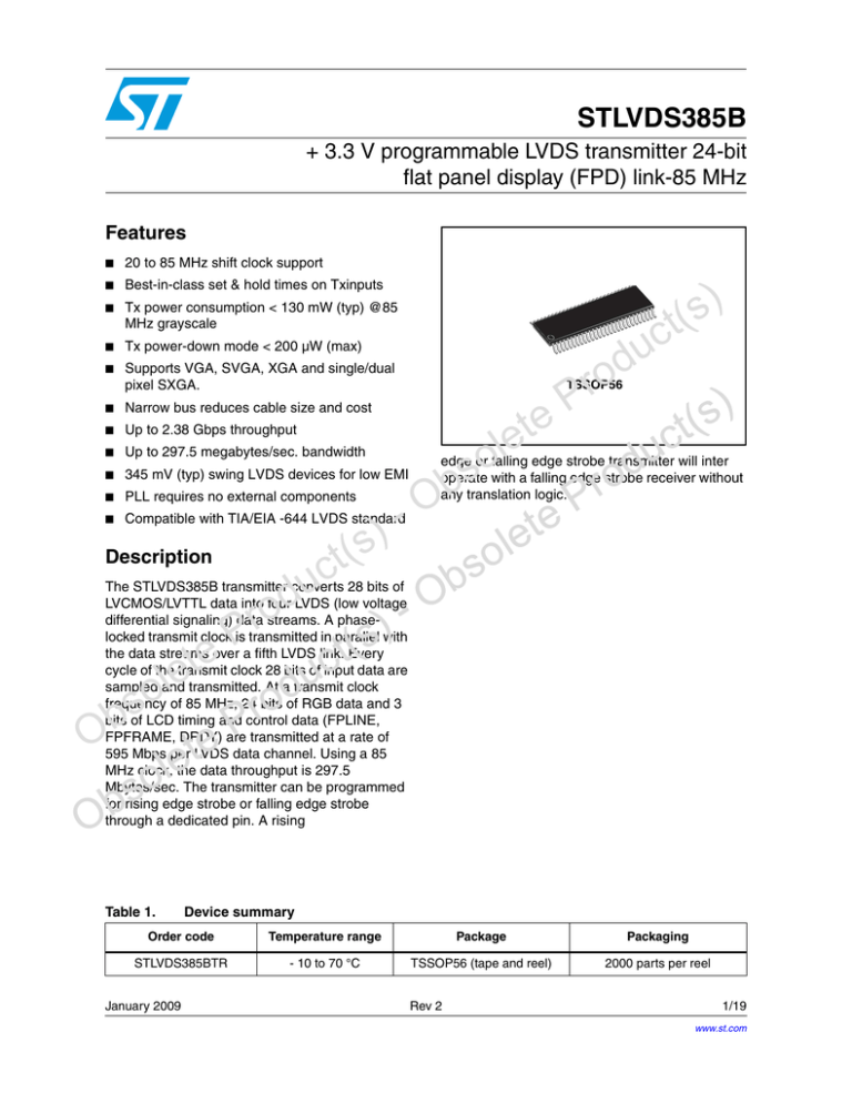
TSSOP56
s
(
t
c
u
d
o
r
eP
t
e
ol
s
b
O
Table 1.
Device summary
Order code
Temperature range
Package
Packaging
STLVDS385BTR
- 10 to 70 °C
TSSOP56 (tape and reel)
2000 parts per reel
January 2009
Rev 2
1/19
www.st.com
19
Contents
STLVDS385B
Contents
1
Pin configuration . . . . . . . . . . . . . . . . . . . . . . . . . . . . . . . . . . . . . . . . . . . . 3
2
Maximum ratings . . . . . . . . . . . . . . . . . . . . . . . . . . . . . . . . . . . . . . . . . . . 5
3
Electrical characteristics . . . . . . . . . . . . . . . . . . . . . . . . . . . . . . . . . . . . . 6
4
AC timing diagrams . . . . . . . . . . . . . . . . . . . . . . . . . . . . . . . . . . . . . . . . . 9
5
Package mechanical data . . . . . . . . . . . . . . . . . . . . . . . . . . . . . . . . . . . . 15
6
Revision history . . . . . . . . . . . . . . . . . . . . . . . . . . . . . . . . . . . . . . . . . . . 18
)
s
t(
c
u
d
e
t
e
l
o
s
)
s
t(
c
u
d
ro
P
e
et
l
o
s
Ob
s
b
O
t
e
ol
2/19
l
o
bs
O
)
s
(
t
c
u
d
o
r
eP
b
O
-
o
r
P
P
e
et
c
u
d
o
r
)
s
t(
STLVDS385B
Pin configuration
1
Pin configuration
Figure 1.
Pin configuration
)
s
t(
c
u
d
e
t
e
l
o
s
)
s
t(
c
u
d
ro
P
e
et
l
o
s
Ob
b
O
-
l
o
bs
o
r
P
)
s
t(
c
u
d
o
r
P
e
et
O
)
s
(
t
c
u
d
o
r
eP
t
e
ol
s
b
O
3/19
Pin configuration
Table 2.
STLVDS385B
Pin description
Pin n°
Symbol
1, 9, 26
VCC
Power supply pins for TTL inputs
2, 3, 4, 6, 7, 8, 10, 11, 12,
14, 15, 16, 18, 19, 20, 22,
23, 24, 25, 27, 28, 30, 50,
51, 52, 54, 55, 56
TXIN
TTL level input. This includes: 8 red, 8 green, 8 blue and 4 control
lines- FPLINE, FPFRAME, and DRDY (also referred to as HSYNC,
VSYNC, data enable)
5, 13, 21, 29
GND
Ground pins for TTL inputs
17
R_FB
Programmable strobe select
31
TxCLKIN
32
PWRDWN
TTL level input. When asserted (low input) tri-states the outputs,
ensuring low current at power down
33, 35
PLL GND
Ground pins for PLL
34
PLL VCC
Power supply pin for PLL
36, 43, 49
LVDS GND
37, 41, 45, 47
TxOUT+
Positive LVDS differential data output
38, 42, 46, 48
TxOUT-
Negative LVDS differential data output
Table 3.
c
u
d
Ground pins for LVDS outputs
e
t
e
l
o
s
TxCLK OUT+ Positive LVDS differential clock output
40
TxCLK OUT-
44
LVDS VCC
b
O
-
R_FB
e
t
le
o
r
P
l
o
bs
c
u
d
o
r
-O
Condition
Strobe status
R_FB = VCC
Rising edge strobe
R_FB = GND or NC
Falling edge strobe
)
s
t(
c
du
o
o
s
r
b
P
O
e
t
e
l
o
s
b
O
)
s
t(
Power supply pin for LVDS outputs
)
s
t(
c
u
d
o
r
P
P
e
et
Negative LVDS differential clock output
Programmable transmitter
R_FB
)
s
t(
TTL level clock input. Pin name TxCLK IN
39
Pin
4/19
Name and function
STLVDS385B
Maximum ratings
2
Maximum ratings
Table 4.
Absolute maximum ratings
Symbol
Value
Unit
- 0.3 to 4
V
CMOS/TTL input voltage
- 0.5 to (VCC + 0.3)
V
VDO
LVDS driver output voltage
- 0.3 to (VCC + 0.3)
V
IOSD
LVDS output short circuit duration
VCC
VI
Parameter
Supply voltage
Continuous
HBM
7
EIAJ
500
)
s
t(
kV
ESD
ILATCH
TJ
TSTG
Note:
Table 5.
Latch up tolerance
± 300
TA
eP
°C
)
s
t(
- 65 to + 150
t
e
l
o
°C
c
u
d
o
r
Absolute maximum ratings are those values beyond which damage to the device may occur.
Functional operation under these condition is not implied.
s
b
O
Recommended operating conditions
Parameter
)-
s
(
t
c
Supply voltage
du
Operating free air temperature
o
r
P
Supply noise voltage
fTxCLKIN
TxCLKIN frequency
e
t
le
c
u
d
)
s
t(
Typ.
Max.
Unit
3.0
3.3
3.6
V
70
°C
100
mVPP
85
MHz
l
o
bs
-O
P
e
et
Min.
0
20
Recommended transmitter input characteristics (VCC = 3.3 V, TJ = - 10 to 70 °C unless
otherwise noted. Typical values are referred to TA = 25 °C)
o
o
s
r
b
P
O
e
t
e
l
o
s
b
O
Symbol
+ 150
Storage temperature range
ΔVCC
Table 6.
mA
ro
Junction temperature
Symbol
VCC
c
u
d
V
Parameter
Min.
Typ.
Max.
Unit
6.0
ns
tCIT
TxCLK IN transition time (Figure 6)
tCIP
TxCLK IN period (Figure 7)
11.76
T
50
ns
tCIH
TxCLK IN high time (Figure 7)
0.35T
0.5T
0.65T
ns
tCIL
TxCLK IN low time (Figure 7)
0.35T
0.5T
0.65T
ns
tXIT
TxIN transition time
6.0
ns
1.0
1.5
5/19
Electrical characteristics
STLVDS385B
3
Electrical characteristics
Table 7.
LVCMOS/LVTTL DC specifications (VCC = 3.3 V, TJ = -10 to 70 °C unless otherwise noted.
Typical values are referred to TA = 25 °C)
Symbol
Parameter
Test conditions
Min.
Typ.
Max.
Unit
VIH
High level input voltage
2.0
VCC
mV
VIL
Low level input voltage
GND
0.8
mV
VCL
Input clamp voltage
-1.5
V
II
ICL = -18mA
VI =0.4 V, 2.5 or VCC
Input current
-10
Parameter
RL = 100Ω
ΔVOD
Change in VOD between
complimentary output
states
RL = 100Ω
VOS
Offset voltage (Note 2)
RL = 100Ω
ΔVOS
Change in VOS between
complimentary output
states
RL = 100Ω
)
s
(
t
c
u
d
o
r
Min.
let
so
b
O
-
Output short circuit current
VO = 0, RL = 100Ω
IOZ
Output tri-state current
Power-down = 0, VO = 0 or VCC
P
e
et
l
o
s
s
(
t
c
u
d
ICCTG
ICCTZ
O
)
)
s
t(
Unit
c
u
d
o
r
mV
eP
1.125
Typ.
345
450
35
mV
1.375
V
35
mV
-3.5
-5
mA
±1
±10
µA
1.25
Transmitter supply current (VCC = 3.3 V, TJ = - 10 to 70 °C unless otherwise noted. Typical
values are referred to TA = 25 °C)
o
r
eP
Parameter
t
e
l
o
s
Ob
µA
Max.
250
t
e
l
o
s
b
IOS
Table 9.
r
P
e
Test conditions
Differential output voltage
ICCTW
ct
0
u
d
o
VOD
Ob
µA
LVDS DC specifications (VCC = 3.3 V, TJ = - 10 to 70 °C unless otherwise noted. Typical
values are referred to TA = 25 °C)
Symbol
Symbol
)
s
(
10
VI = GND
Table 8.
6/19
-0.79
Transmitter supply current
worst case
Transmitter supply current
16 grayscale
Transmitter supply current
power down
Test conditions
RL = 100Ω, CL = 5pF,
worst case pattern
(Figure 2, Figure 4)
RL = 100Ω, CL = 5pF,
16 grayscale pattern
(Figure 2, Figure 4)
Min.
Typ.
Max.
f = 32.5 MHz
31
45
f = 40 MHz
32
50
f = 65 MHz
37
55
f = 85 MHz
42
60
f = 32.5 MHz
29
38
f = 40 MHz
30
40
f = 65 MHz
35
45
f = 85 MHz
39
50
10
55
Unit
mA
mA
Power-down = low
driver outputs in tri-state under
power-down mode
µA
STLVDS385B
Table 10.
Electrical characteristics
Transmitter switching characteristics (VCC = 3.3 V, TJ = -10 to 70 °C unless otherwise
noted. Typical values are referred to TA = 25 °C)
Symbol
Parameter
Test conditions
Min.
Typ.
Max.
Unit
tLLHT
LVDS low-to-high transition time
(Figure 5)
0.75
1.5
ns
tLLLT
LVDS high-to-low transition time
(Figure 5)
0.75
1.5
ns
tTPP0
Transmitter output pulse position for bit 0
(Figure 12 - Note 3)
-0.25
0
0.25
ns
tTPP1
Transmitter output pulse position for bit 1
3.32
3.57
3.82
ns
tTPP2
Transmitter output pulse position for bit 2
6.89
7.14
7.39
ns
10.46
10.71
10.96
ns
ns
f = 40 MHz
)
s
t(
c
u
d
tTPP3
Transmitter output pulse position for bit 3
tTPP4
Transmitter output pulse position for bit 4
14.04
14.29
14.54
tTPP5
Transmitter output pulse position for bit 5
17.61
17.86
18.11
ns
tTPP6
Transmitter output pulse position for bit 6
21.18
21.43
21.68
ns
tTPP0
Transmitter output pulse position for bit 0
(Figure 12 - Note 3)
eP
tTPP1
Transmitter output pulse position for bit 1
tTPP2
Transmitter output pulse position for bit 2
Transmitter output pulse position for bit 3
tTPP4
Transmitter output pulse position for bit 4
tTPP5
Transmitter output pulse position for bit 5
tTPP6
Transmitter output pulse position for bit 6
tTPP0
Transmitter output pulse position for bit 0
(Figure 12 - Note 3)
ct
let
tTPP1
so
tTPP2
r
P
e
c
u
d
t
e
l
o
)
(s
tTPP3
u
d
o
ro
)
s
t(
s
b
O
-O
Transmitter output pulse position for bit 1
Transmitter output pulse position for bit 2
o
r
eP
Ob t
le
o
s
b
O
0
0.20
ns
2.20
2.40
ns
4.40
4.60
ns
6.39
6.59
6.79
ns
8.59
8.79
8.99
ns
10.79
10.99
11.19
ns
12.99
13.19
13.99
ns
-0.20
0
0.20
ns
1.48
1.68
1.88
ns
3.16
3.36
3.56
ns
4.84
5.04
5.24
ns
2.00
eP
let
o
s
b
f = 85 MHz
c
u
d
o
r
-0.20
4.20
f = 65 MHz
)
s
t(
tTPP3
Transmitter output pulse position for bit 3
tTPP4
Transmitter output pulse position for bit 4
6.52
6.72
6.92
ns
tTPP5
Transmitter output pulse position for bit 5
8.20
8.40
8.60
ns
tTPP6
Transmitter output pulse position for bit 6
9.88
10.08
10.28
ns
tSTC
TxIN setup to TxCLK IN (Figure 7)
2.5
ns
tHTC
TxIN hold to TxCLK IN (Figure 7)
0
ns
tCCD
TxCLK IN to TxCLK OUT delay (Figure 8) TA = 25°C, VCC = 3.3V
3.8
6.3
ns
tCCD
TxCLK IN to TxCLK OUT delay (Figure 8)
2.8
7.1
ns
tJCC
f = 85 MHz
Transmitter jitter cycle-to-cycle (Figure 12
f = 65 MHz
- Note 4)
f = 40 MHz
110
150
210
230
350
370
ps
7/19
Electrical characteristics
Table 10.
STLVDS385B
Transmitter switching characteristics (continued) (VCC = 3.3 V, TJ = -10 to 70 °C unless
otherwise noted. Typical values are referred to TA = 25 °C)
Symbol
Parameter
tPLLS
tPDD
Note:
Max.
Unit
Transmitter phase lock loop set (Figure 9)
10
ms
Transmitter power down delay (Figure 11)
100
ns
2
VOS previously referred as VCM.
3
The minimum and maximum limits are based on statistical analysis of the device
performance over process, voltage, and temperature range. This parameter is functionality
tested only on automatic test equipment (ATE).
4
The limits are based on bench characterization of the device’s jitter response over the power
supply voltage range. Output clock jitter is measured with a cycle-to-cycle jitter of ± 3 ns
applied to the input clock signal while data inputs are switching. A jitter event of 3 ns,
represents worse case jump in the clock edge from most graphics controller VGA chips
currently available.
)
s
t(
c
u
d
e
t
e
l
o
s
o
r
P
c
u
d
o
r
)
s
t(
5
The worst case test pattern produces a maximum toggling of digital circuits, LVDS I/O and
CMOS/TTL I/O.
6
The 16 grayscale test pattern tests device power consumption for a “typical” LCD display
pattern. The test pattern approximates signal switching needed to produce groups of 16
vertical stripes across the display.
7
Figure 2, Figure 3 show a falling edge data strobe (TxCLK IN/RxCLK OUT).
8
Recommended pin to signal mapping. Customer may choose to define differently.
)
s
t(
l
o
s
8/19
Typ.
Current into device pins is defined as positive. Current out of device pins is defined as
negative. Voltages are referenced to ground unless otherwise specified (except VOD and
ΔVOD).
P
e
et
c
u
d
b
O
-
l
o
bs
O
)
s
(
t
c
u
d
o
r
eP
t
e
ol
s
b
O
Min.
1
ro
Ob
Test conditions
P
e
et
STLVDS385B
AC timing diagrams
4
AC timing diagrams
Figure 2.
Worst case test pattern (1)
)
s
t(
c
u
d
e
t
e
o
r
P
1. The worst case test pattern produces a maximum toggling of digital circuits, LVDS I/O and CMOS/TTL I/O.
l
o
s
)
s
t(
c
u
d
ro
P
e
et
l
o
s
Ob
b
O
-
l
o
bs
)
s
t(
c
u
d
o
r
P
e
et
O
)
s
(
t
c
u
d
o
r
eP
t
e
ol
s
b
O
9/19
AC timing diagrams
STLVDS385B
16 grayscale test patter (1) (2) (3)
Figure 3.
)
s
t(
c
u
d
e
t
e
l
o
s
)
s
t(
c
u
d
ro
P
e
et
l
o
s
Ob
b
O
-
l
o
bs
o
r
P
c
u
d
o
r
P
e
et
O
)
s
(
t
c
u
d
o
r
eP
t
e
ol
s
b
O
1. The 16 grayscale test pattern tests device power consumption for a “typical” LCD display pattern. The test pattern
approximates signal switching needed to produce groups of 16 vertical stripes across the display.
2. Figure 2, Figure 3 show a falling edge data strobe (TxCLK IN/RxCLK OUT).
3. Recommended pin to signal mapping. Customer may choose to define differently.
10/19
)
s
t(
STLVDS385B
Figure 4.
AC timing diagrams
Figure 5.
(Transmitter) LVDS output load
)
s
t(
c
u
d
(Transmitter) LVDS transition time
e
t
e
l
o
s
)
s
t(
Figure 6.
ro
l
o
bs
)
s
t(
c
u
d
o
r
P
e
et
O
)
(Transmitter) input clock transition time
P
e
et
l
o
s
Ob
c
u
d
b
O
-
o
r
P
s
(
t
c
u
d
o
r
eP
t
e
ol
s
b
O
11/19
AC timing diagrams
Figure 7.
STLVDS385B
(Transmitter) setup/hold and high/low times (falling edge strobe)
)
s
t(
c
u
d
e
t
e
l
o
s
)
s
t(
Figure 8.
(Transmitter) clock in to clock out delay
c
u
d
ro
P
e
et
l
o
s
Ob
12/19
l
o
bs
O
)
s
(
t
c
u
d
o
r
eP
t
e
ol
s
b
O
b
O
-
o
r
P
P
e
et
c
u
d
o
r
)
s
t(
STLVDS385B
Figure 9.
AC timing diagrams
(Transmitter) phase lock loop set time
)
s
t(
c
u
d
e
t
e
l
o
s
b
O
-
c
u
d
ro
P
e
et
l
o
s
Ob
l
o
bs
)
s
t(
c
u
d
o
r
P
e
et
Figure 10. 28 parallel TTL data inputs mapped to LVDS outputs
)
s
t(
o
r
P
O
)
s
(
t
c
u
d
o
r
eP
t
e
ol
s
b
O
13/19
AC timing diagrams
STLVDS385B
Figure 11. Transmitter power down delay
)
s
t(
c
u
d
e
t
e
Figure 12. Transmitter LVDS output pulse position measurement
l
o
s
)
s
t(
c
u
d
ro
P
e
et
l
o
s
Ob
s
b
O
t
e
ol
14/19
l
o
bs
O
)
s
(
t
c
u
d
o
r
eP
b
O
-
o
r
P
P
e
et
c
u
d
o
r
)
s
t(
STLVDS385B
5
Package mechanical data
Package mechanical data
In order to meet environmental requirements, ST offers these devices in different grades of
ECOPACK® packages, depending on their level of environmental compliance. ECOPACK®
specifications, grade definitions and product status are available at: www.st.com.
ECOPACK® is an ST trademark.
)
s
t(
c
u
d
e
t
e
l
o
s
)
s
t(
c
u
d
ro
P
e
et
l
o
s
Ob
b
O
-
l
o
bs
o
r
P
)
s
t(
c
u
d
o
r
P
e
et
O
)
s
(
t
c
u
d
o
r
eP
t
e
ol
s
b
O
15/19
Package mechanical data
STLVDS385B
TSSOP56 mechanical data
mm.
inch.
Dim.
Min.
Typ.
Max.
A
Min.
Max.
1.2
A1
0.05
0.047
0.15
A2
0.002
0.006
0.9
0.17
0.27
0.0067
c
0.09
0.20
0.0035
D
13.9
14.1
0.547
E
7.95
8.25
0.313
E1
6.0
6.2
e
0°
L
0.45
)
s
(
t
c
u
d
o
r
P
e
et
A2
A
l
o
s
A1
bs
o
r
eP
e
o
r
P
0.011
0.0079
0.555
)
s
t(
0.325
c
u
d
o
r
0.244
0.0197 BSC
eP
0°
t
e
l
o
s
b
0.75
0.020
O
)
s
(
t
c
u
d
b
e
t
e
ol
-O
8°
c
u
d
0.236
0.5 BSC
K
)
s
t(
0.035
b
Ob
Typ.
K
8°
0.030
L
E
c
D
t
e
ol
s
b
O
E1
PIN 1 IDENTIFICATION
1
7065590B
16/19
STLVDS385B
Package mechanical data
Tape and reel TSSOP56 mechanical data
mm.
inch.
Dim.
Min.
Typ.
Max.
A
Min.
Max.
330
12.992
C
12.8
D
20.2
0.795
N
60
2.362
13.2
T
0.504
0.519
8.7
8.9
0.342
Bo
17.2
17.4
0.677
Ko
1.4
1.6
0.055
Po
3.9
4.1
0.153
P
11.9
12.1
)
s
t(
c
u
d
ro
P
e
et
l
o
s
e
t
e
l
o
s
od
Pr
l
o
bs
1.197
0.350
0.685
)
s
t(
0.063
c
u
d
o
r
0.468
b
O
-
)
s
t(
uc
30.4
Ao
Ob
Typ.
0.161
0.476
P
e
et
O
)
s
(
t
c
u
d
o
r
eP
t
e
ol
s
b
O
17/19
Revision history
STLVDS385B
6
Revision history
Table 11.
Document revision history
Date
Revision
Changes
21-Jun-2004
1
First release.
26-Jan-2009
2
Modified Table 1 on page 1.
)
s
t(
c
u
d
e
t
e
l
o
s
)
s
t(
c
u
d
ro
P
e
et
l
o
s
Ob
s
b
O
t
e
ol
18/19
l
o
bs
O
)
s
(
t
c
u
d
o
r
eP
b
O
-
o
r
P
P
e
et
c
u
d
o
r
)
s
t(
STLVDS385B
)
s
t(
Please Read Carefully:
c
u
d
Information in this document is provided solely in connection with ST products. STMicroelectronics NV and its subsidiaries (“ST”) reserve the
right to make changes, corrections, modifications or improvements, to this document, and the products and services described herein at any
time, without notice.
All ST products are sold pursuant to ST’s terms and conditions of sale.
e
t
e
o
r
P
)
s
t(
Purchasers are solely responsible for the choice, selection and use of the ST products and services described herein, and ST assumes no
liability whatsoever relating to the choice, selection or use of the ST products and services described herein.
l
o
s
c
u
d
o
r
No license, express or implied, by estoppel or otherwise, to any intellectual property rights is granted under this document. If any part of this
document refers to any third party products or services it shall not be deemed a license grant by ST for the use of such third party products
or services, or any intellectual property contained therein or considered as a warranty covering the use in any manner whatsoever of such
third party products or services or any intellectual property contained therein.
)
s
t(
b
O
-
l
o
bs
P
e
et
UNLESS OTHERWISE SET FORTH IN ST’S TERMS AND CONDITIONS OF SALE ST DISCLAIMS ANY EXPRESS OR IMPLIED
WARRANTY WITH RESPECT TO THE USE AND/OR SALE OF ST PRODUCTS INCLUDING WITHOUT LIMITATION IMPLIED
WARRANTIES OF MERCHANTABILITY, FITNESS FOR A PARTICULAR PURPOSE (AND THEIR EQUIVALENTS UNDER THE LAWS
OF ANY JURISDICTION), OR INFRINGEMENT OF ANY PATENT, COPYRIGHT OR OTHER INTELLECTUAL PROPERTY RIGHT.
c
u
d
O
)
UNLESS EXPRESSLY APPROVED IN WRITING BY AN AUTHORIZED ST REPRESENTATIVE, ST PRODUCTS ARE NOT
RECOMMENDED, AUTHORIZED OR WARRANTED FOR USE IN MILITARY, AIR CRAFT, SPACE, LIFE SAVING, OR LIFE SUSTAINING
APPLICATIONS, NOR IN PRODUCTS OR SYSTEMS WHERE FAILURE OR MALFUNCTION MAY RESULT IN PERSONAL INJURY,
DEATH, OR SEVERE PROPERTY OR ENVIRONMENTAL DAMAGE. ST PRODUCTS WHICH ARE NOT SPECIFIED AS "AUTOMOTIVE
GRADE" MAY ONLY BE USED IN AUTOMOTIVE APPLICATIONS AT USER’S OWN RISK.
ro
P
e
et
l
o
s
s
(
t
c
u
d
Resale of ST products with provisions different from the statements and/or technical features set forth in this document shall immediately void
any warranty granted by ST for the ST product or service described herein and shall not create or extend in any manner whatsoever, any
liability of ST.
Ob
t
e
ol
o
r
eP
s
b
O
ST and the ST logo are trademarks or registered trademarks of ST in various countries.
Information in this document supersedes and replaces all information previously supplied.
The ST logo is a registered trademark of STMicroelectronics. All other names are the property of their respective owners.
© 2009 STMicroelectronics - All rights reserved
STMicroelectronics group of companies
Australia - Belgium - Brazil - Canada - China - Czech Republic - Finland - France - Germany - Hong Kong - India - Israel - Italy - Japan Malaysia - Malta - Morocco - Singapore - Spain - Sweden - Switzerland - United Kingdom - United States of America
www.st.com
19/19
