P-Channel
CICLON NexFET™ Power MOSFETs
CSD25301W1015
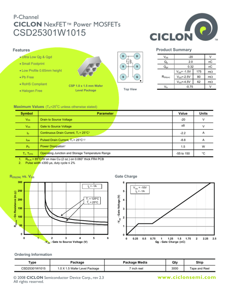
Product Summary
Features
• Ultra Low Qg & Qgd
D
D
• Small Footprint
S
S
• RoHS Compliant
nC
0.32
nC
VGS= -1.5V
175
mΩ
VGS=-2.5V
80
mΩ
VGS=-4.5V
62
mΩ
Vth
Top View
Level Package
V
2.0
RDS(on)
G
CSP 1.0 x 1.5 mm Wafer
• Halogen Free
-20
Qg
Qgd
S
• Low Profile 0.65mm height
• Pb Free
VDS
-0.75
V
Maximum Values (TA=25oC unless otherwise stated)
Symbol
Parameter
Units
VDS
Drain to Source Voltage
-20
V
VGS
Gate to Source Voltage
±8
V
ID
Continuous Drain Current, TJ = 25°C1
-2.2
A
IDM
Pulsed Drain Current, TJ = 25°C1,2
-8.8
A
PD
Power Dissipation1
1.5
W
-55 to 150
°C
Operating Junction and Storage Temperature Range
TJ, TSTG
0
1.
2.
RthJA = 85 C/W on max Cu (2 oz.) on 0.060” thick FR4 PCB
Pulse width ≤300 µs, duty cycle ≤ 2%
RDS(ON) vs. VGS
Gate Charge
300
6
ID = -1A
250
V DS = -10V
ID = -1A
5
-V GS - Gate Voltage (V)
RDS(on) - On Resistance (m Ω )
Value
TJ = 125ºC
TJ = 25ºC
200
150
100
50
4
3
2
1
0
0
0
1
-V GS
2
3
4
- Gate to Source Voltage (V)
5
6
0
0.25
0.5
0.75
1
1.25
1.5
1.75
Qg - Gate Charge (nC)
2
2.25
2.5
Ordering Information
Type
CSD25301W1015
Package
1.0 X 1.5 Wafer Level Package
© 2008 CICLON Semiconductor Device Corp., rev 2.3
All rights reserved.
Package Media
7 inch reel
Qty
Ship
3000
Tape and Reel
www.ciclonsemi.com
P-Channel
CICLON NexFET™ Power MOSFETs
CSD25301W1015
Electrical Characteristics (TA = 25OC unless otherwise stated)
Symbol
Parameter
Test Conditions
Min
Typ
Max
Units
Drain to Source Voltage
VGS = 0V, ID = -250µA
-20
▬
▬
V
IDSS
Drain to Source Leakage Current
VGS = 0V, VDS = -16V
▬
▬
-1
µA
IGSS
Gate to Source Leakage Current
VDS = 0V, VGS = ±8V
▬
▬
-100
nA
VDS = VGS, ID = -250µA
-0.4
-0.75
-1.0
V
VGS = -1.5V, ID = -1A
▬
175
220
mΩ
VGS = -2.5V, ID = -1A
▬
80
100
mΩ
VGS = -4.5V, ID = -1A
▬
62
75
mΩ
VDS = -10V, ID = -1A
▬
5.8
▬
S
▬
210
270
pF
▬
90
120
pF
▬
30
40
pF
▬
1.9
2.5
nC
▬
0.4
▬
nC
▬
0.35
▬
nC
▬
0.17
▬
nC
▬
1.7
▬
nC
▬
4.0
▬
ns
▬
2.0
▬
ns
▬
29
▬
ns
▬
12
▬
ns
▬
-0.75
-1.0
V
▬
0.9
▬
nC
▬
8.2
▬
ns
Static Characteristics
BVDSS
VGS(th)
RDS(on)
gfs
Gate to Source Threshold Voltage
Drain to Source On Resistance
Transconductance
Dynamic Characteristics
CISS
Input Capacitance
COSS
Output Capacitance
CRSS
Reverse Transfer Capacitance
Qg
Gate Charge Total (-4.5V)
Qgd
Gate Charge Gate to Drain
Qgs
Gate Charge Gate to Source
Qg(th)
Gate Charge at Vth
QOSS
Output Charge
td(on)
Turn On Delay Time
tr
td(off)
tf
Rise Time
Turn Off Delay Time
Fall Time
VGS = 0V, VDS = -10V
f = 1MHz
VDS = -10V, ID = -1A
VDS = -9.8V, VGS = 0V
VDS = -10V
VGS = -4.5V ID = -1A
RG = 20Ω
Diode Characteristics
VSD
Diode Forward Voltage
Qrr
Reverse Recovery Charge
trr
Reverse Recovery Time
© 2008 CICLON Semiconductor Device Corp., rev 2.3
All rights reserved.
IS = -1A, VGS = 0V
Vdd=-9.8V, IF = -1A,
di/dt = 200A/µs
Vdd=-9.8V, IF = -1A,
di/dt = 200A/µs
www.ciclonsemi.com
P-Channel
CICLON NexFET™ Power MOSFETs
CSD25301W1015
Thermal Characteristics (TA = 25OC unless otherwise stated)
Symbol
Parameter
Min
Typ
Max
Units
Thermal Characteristics
R θJA
Thermal Resistance Junction to Ambient (Minimum Cu area)
▬
▬
270
°C/W
R θJA
Thermal Resistance Junction to Ambient (1 in2 Cu area)
▬
▬
105
°C/W
o
Max Rθja =105 C/W
o
Max Rθja =270 C/W when
2
when mounted on 1in of
mounted on min pad area of
2 oz. Cu.
2 oz. Cu.
ZthJA Normalized thermal impedance
10
1
0 .5
0 .3
0.1
0.01
0 .1
0 .0 5
0 .0 2
0 .0 1
Duty Cycle =t1/t2
P
t1
t2
0.001
0.0001
1.E-05
RthJA =850C/W (1in2 Cu)
Si n g l e Pu l se
1.E-04
Tj = P * ZthJA * RthJA
1.E-03
1.E-02
1.E-01
Pulse duration (s)
1.E+00
1.E+01
1.E+02
1.E+03
Figure 1: Transient Thermal Impedance
© 2008 CICLON Semiconductor Device Corp., rev 2.3
All rights reserved.
www.ciclonsemi.com
P-Channel
CICLON NexFET™ Power MOSFETs
CSD25301W1015
Typical MOSFET Characteristics (TA = 25oC unless otherwise stated)
4.5
8.0
4.0
V GS
V GS
V GS
V GS
V GS
7.0
6.0
5.0
4.0
-ID - Drain Current (A)
5.0
9.0
-ID - Drain Current (A)
10.0
= -4.5V
= -3.0V
= -2.5V
= -2.0V
= -1.5V
3.0
3.5
3.0
2.5
1.5
1.0
1.0
0.5
0.0
0.5
-V DS
1.0
1.5
2.0
- Drain to Source Voltage (V)
2.5
TJ = -55ºC
TJ = 25ºC
TJ = 125ºC
2.0
2.0
0.0
V DS = -5V
0.0
0.75
3.0
Figure 2: Saturation Characteristics
2
300
V GS = 0V, f = 1MHz
V DS = -10V
ID = -1A
250
Capacitance (pF)
5
4
3
2
200
CISS = CGD+CGS
COSS =CDS+CGD
CRSS = CGD
150
100
50
1
0
0
0
0.25
0.5
0.75
1
1.25
1.5
1.75
Qg - Gate Charge (nC)
2
2.25
0
2.5
5
10
15
-V DS - Drain to Source Voltage (V)
Figure 4: Gate Charge
20
Figure 5: Capacitance
1.0
300
ID = -250µA
0.9
ID = -1A
0.8
RDS(on) - On Resistance (m Ω )
-V GS(th) - Threshold Voltage (V)
1.25
1.5
1.75
-V GS - Gate to Source Voltage (V)
Figure 3: Transfer Characteristics
6
-V GS - Gate Voltage (V)
1
0.7
0.6
0.5
0.4
0.3
0.2
250
TJ = 125ºC
TJ = 25ºC
200
150
100
50
0.1
0.0
-75
0
-25
25
75
125
TJ - Junction Tem perature (°C)
Figure 6: Threshold Voltage vs. Temperature
© 2008 CICLON Semiconductor Device Corp., rev 2.3
All rights reserved.
175
0
1
2
3
4
-V GS - Gate to Source Voltage (V)
5
6
Figure 7: On Resistance vs. Gate Voltage
www.ciclonsemi.com
P-Channel
CICLON NexFET™ Power MOSFETs
CSD25301W1015
Typical MOSFET Characteristics (TA = 25oC unless otherwise stated)
10
1.6
Normalized On Resistance
1.4
-ISD - Source to Drain Current (A)
ID = -1A, V GS = -4.5V
1.2
1.0
0.8
0.6
0.4
0.2
0.0
-75
1
TJ = 125ºC
TJ = 25ºC
0.1
0.01
0.001
0.0001
-25
25
75
T J - Junction Tem perature (°C)
125
175
0.0
Figure 8: On Resistance vs. Temperature
0.2
0.4
0.6
0.8
-V SD - Source to Drain Voltage (V)
1.0
1.2
Figure 9: Typical Diode Forward Voltage
100
2.5
-ID - Drain Current (A)
-ID - Drain Current (A)
2.0
10
100us
1
1ms
0.1
May be limited by
Rds (ON)
10ms
Single pulse
RthJA =2160C/W (min Cu)
1.0
0.5
100ms
DC
0.01
0.1
1.5
1
10
-V DS - Drain Voltage (V)
Figure 10: Maximum Safe Operating Area
© 2008 CICLON Semiconductor Device Corp., rev 2.3
All rights reserved.
100
0.0
-50
-25
0
25
50
75
100
125
TJ - Junction Tem perature (°C)
150
175
Figure 11: Maximum Drain Current vs. Temperature
www.ciclonsemi.com
P-Channel
CICLON NexFET™ Power MOSFETs
CSD25301W1015
CSD25301W1015 Package Dimensions
Top View
Bottom View
Notes:
1. All Dimensions are in
mm
Pinout
A
B
C
© 2008 CICLON Semiconductor Device Corp., rev 2.3
All rights reserved.
1
G
S
D
2
S
S
D
www.ciclonsemi.com
P-Channel
CICLON NexFET™ Power MOSFETs
CSD25301W1015
Tape and Reel Information
PIN 1
IDENTIFIER
Package Marking Information
Location:
1st Line
Product Code = 75301 (Fixed Text)
2nd Line
25301
XXXXWW
XXXXWW = Last 4 digits of lot number
(XXXX); Wafer number (WW)
C
PIN 1
IDENTIFIER
© 2008 CICLON Semiconductor Device Corp., rev 2.3
All rights reserved.
Y
www.ciclonsemi.com
C
P-Channel
CICLON NexFET™ Power MOSFETs
CSD25301W1015
Disclaimer
CICLON Semiconductor Device Corp. (“CICLON”) reserves the right to make corrections, modifications, enhancements, improvements and other
changes to its products and services at any time and to discontinue any product or service without notice. Customers should obtain the latest relevant
information before placing orders and should verify that such information is current and complete. All products are sold subject to CICLON’s terms and
conditions of sale supplied at the time of order acknowledgement.
Additional Information
For further information on technology, delivery terms and conditions, or pricing please contact your nearest CICLON Semiconductor representative.
CICLON Semiconductor Device Corp.
116 Research Drive, Bethlehem, PA 18015
T 610-849-5100 F 610-849-5101
© 2008 CICLON Semiconductor Device Corp., rev 2.3
All rights reserved.
www.ciclonsemi.com
