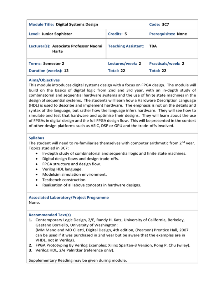
Module Title: Digital Systems Design
Code: 3C7
Level: Junior Sophister
Credits: 5
Prerequisites: None
Lecturer(s): Associate Professor Naomi
Harte
Teaching Assistant:
TBA
Terms: Semester 2
Lectures/week: 2
Practicals/week: 2
Duration (weeks): 12
Total: 22
Total: 22
Aims/Objectives
This module introduces digital systems design with a focus on FPGA design. The module will
build on the basics of digital logic from 2nd and 3rd year, with an in-depth study of
combinatorial and sequential hardware systems and the use of finite state machines in the
design of sequential systems. The students will learn how a Hardware Description Language
(HDL) is used to describe and implement hardware. The emphasis is not on the details and
syntax of the language, but rather how the language infers hardware. They will see how to
simulate and test that hardware and optimise their designs. They will learn about the use
of FPGAs in digital design and the full FPGA design flow. This will be presented in the context
of other design platforms such as ASIC, DSP or GPU and the trade-offs involved.
Syllabus
The student will need to re-familiarise themselves with computer arithmetic from 2nd year.
Topics studied in 3C7:
In-depth study of combinatorial and sequential logic and finite state machines.
Digital design flows and design trade-offs.
FPGA structure and design flow.
Verilog HDL language.
Modelsim simulation environment.
Testbench construction.
Realisation of all above concepts in hardware designs.
Associated Laboratory/Project Programme
None.
Recommended Text(s)
1. Contemporary Logic Design, 2/E, Randy H. Katz, University of California, Berkeley,
Gaetano Borriello, University of Washington:
(MM Mano and MD Ciletti, Digital Design, 4th edition, (Pearson) Prentice Hall, 2007.
can be used if it was purchased in 2nd year but be aware that the examples are in
VHDL, not in Verilog).
2. FPGA Prototyping By Verilog Examples: Xilinx Spartan-3 Version, Pong P. Chu (wiley).
3. Verilog HDL, 2/e Palnitkar (reference only).
Supplementary Reading may be given during module.
Learning Outcomes
On completion of this module the student will be able to:
1. Discriminate between combinatorial and sequential circuits.
2. Design state machines to control complex systems.
3. Define and describe digital design flows for system design and recognise the trade-offs
involved in different approaches.
4. Write synthesisable verilog.
5. Write a verilog testbench to test verilog modules.
6. Analyse code coverage of a verilog testbench.
7. Target a verilog design to an FPGA board.
8. Analyse and debug verilog modules.
9. Build a synchronous DSP system in verilog and verify its performance.
Teaching Strategies
This is a highly practical module. There will be 2 “classic” style lectures per week. There
will also be a two-hour practical session each week which will be a lecture-come-lab,
where the lecturer will talk about the content of the session and the student will “learn by
doing”. The FPGA board used to support the practical sessions is the Spartan-3 starter
board. The practical sessions will require the students to complete the weekly assignment
outside class hours (average 4 extra hours per assignment, 9 assignments in total),
spreading the load through the year. It is critical that the student keeps up with the
practical work during the semester.
Assessment Mode(s)
The written examination and the module practical work will each contribute 50% of the
overall module mark at the Annual Examination. The practical element of the module
CANNOT be repeated.
Attendance at weekly practical sessions is COMPULSORY. No marks will be given for the
corresponding assignment for unattended practical sessions.
Submission dates will be given for each related assignment.
Late assignments policy:
• Lose half of marks if up to 1 week late.
• No marks if over 1 week late.


